CSCI-UA.0436 Computer Architecture
2018-19 Fall
Allan Gottlieb
Tuesday Thursday 3:30-4:45
Room 512 CIWW
Start Lecture #1
Chapter 0: Administrivia
I start at Chapter 0 so that when we get to chapter 1, the
numbering will agree with the text.
0.1: Contact Information
- email: my-last-name AT nyu DOT edu (best method)
- web: cs.nyu.edu/~gottlieb
- office: 60 Fifth ave, Room 316
- office phone: 212 998 3344
0.2: Course Web Page
There is a web site for the course.
You can find it from my home page, which is listed above, or from
the department's home page.
- You can find these lecture notes on the course home page.
Please let me know if you can't find them.
- The notes are updated as bugs are found or improvements made.
As a result, I do not recommend printing the notes now (if at
all).
- I will place markers at the end of each lecture after the
lecture is given.
For example, the
Start Lecture #1
marker above can be
thought of as End Lecture #0
.
0.3: Textbook
The course text is Hennessy and Patterson,
Computer Organization and Design: The Hardware/Software Interface,
5th edition, which I will refer to as 5e.
- Available in the bookstore.
- The main body of the book assumes you have had a full course
in logic design.
- I do NOT make that strong an assumption.
I just assume you had 201.
- We will start with appendix B, which is a logic design review.
However since 201 is a prerequisite, we will go rather quickly
over some parts.
- Many of the figures in these notes are based on figures from
the course textbook.
Although I have personally redrawn all the figures (except for
two pictures on carry lookahead adders), the following copyright
notice (from Morgan Kaufman / Elsevier) probably applies (IANAL).
All figures from Computer Organization and Design: The
Hardware/Software Approach, Fourth Edition, by David Patterson
and John Hennessy, are copyrighted material (copyright 2009 by
Elsevier inc inc. all rights reserved).
Figures may be reproduced only for classroom or personal
educational use in conjunction with the book and only when the
above copyright line is included.
They may not be otherwise reproduced, distributed, or
incorporated into other works without the prior written consent
of the publisher.
0.4 Email, and the Mailman Mailing List
- You should have all been automatically added to the mailing list
for this course and should have received a test message from
me.
- Mail to the list should be sent to arch-FA18-????@nyu.edu.
- Membership on the list is required; I assume
that messages I send to the mailing list are read.
- If you want to send mail just to me, use my-last-name AT nyu DOT
edu not the mailing list.
- Questions on the labs should go to the mailing list.
You may answer questions posed on the list as well.
Note that replies are sent to the list.
- I will respond to all questions sent to the list.
If another student has answered the question before I get to it, I
will confirm if the answer given is correct.
- Please use proper mailing list etiquette.
- Send plain text messages rather than (or at
least in addition to) html.
- Use
Reply
to contribute to the current thread,
but NOT to start another topic.
- If quoting a previous message, trim off irrelevant parts.
- Use a descriptive Subject: field when starting a new topic.
- Do not use one message to ask two unrelated questions.
- As you will see, when I respond to a message, I either place my
reply after the original text or interspersed with it (rather than
putting the reply at the top).
This preference is most relevant for detailed questions that lead
to serious conversations involving many messages.
I find it quite useful when reviewing a serious conversations to
have the entire conversation in chronological order.
I believe you would also find it useful when reviewing for an
exam.
(-0).5 Grades
Grades are based on the labs and exams; the weighting will be
approximately
25%*LabAverage + 30%*MidtermExam + 45%*FinalExam
(but see homeworks below).
0.6: The Upper Left Board
I use the upper left board for lab/homework assignments and
announcements.
I should never erase that board.
If you see me start to erase an announcement, please let me know.
I try very hard to remember to write all announcements on the upper
left board and I am normally successful.
If, during class, you see that I have forgotten to record something,
please let me know.
HOWEVER, even if I forgot and no one reminds me,
the assignment has still been given.
0.7: Homeworks and Labs
I make a distinction between homeworks and labs.
Labs are
- Required.
- Usually computer programs you must write.
In this course, the
programming language
is a graphical
language for drawing electronic circuits and simulating their
behavior.
- Due several lectures later (date given on assignment).
- Given in the notes and on NYU Classes with supplemental material
on separate web pages.
Your solution is submitted via NYU Classes.
- Graded and form part of your final grade.
- Penalized for lateness.
- The penalty is 1 point per day up to 30 days; then 3 points
per day.
- This penalty is much too mild; but it is
enforced.
- Later in the semester firm deadlines will
be set after which no labs will be accepted.
Please do not ignore these deadlines.
Repeat: the deadlines to be given later in the semester are
FIRM
Homeworks are
- Optional.
- Due the beginning of the Next lecture.
- Not accepted late.
- Mostly from the book.
- The assignment is given in the notes and Classes; your solution
is submitted via NYU Classes.
- Checked for completeness and graded 0/1/2.
- Able to help, but not hurt, your final grade.
0.7.1: Homework Numbering
Homeworks are numbered by the class in which they are assigned.
So any homework given today is homework #1.
Even if I do not give homework today, the homework assigned next
class will be homework #2.
Unless I explicitly state otherwise, all homeworks assignments can
be found in the class notes.
So the homework present in the notes for lecture #n is homework #n
(even if I inadvertently forgot to write it to the upper left
board).
0.7.2: Doing Labs on non-NYU Systems
This course will have graphical labs so I expect you will
work on your personal computers.
You will submit your labs via NYU Classes.
0.7.3: Obtaining Help with the Labs
Good methods for obtaining help include
- Asking me during office hours (see web page for my hours).
- Asking the mailing list.
- Asking another student.
- But ...
Your lab must be your own.
That is, each student must submit a unique lab.
0.7.4: Computer Language Used for Labs
Most if not all labs will be in logisim, a graphical language for
drawing electronic circuits and simulating their behavior.
I do not assume you know logisim now.
I will demo it a little but expect you to learn it via the online
help (that is how I learned it).
0.7.5: Resubmitting Homeworks and Labs
You may resubmit a homework a few times until the deadline.
You may resubmit a lab a few times until your lab has been returned
by the grader, after which resubmissions are not permitted.
0.8: A Grade of Incomplete
The rules for incompletes and grade changes are set by the school
and not the department or individual faculty member.
The rules set by CAS can be found
here.
They state:
The grade of I (Incomplete) is a temporary grade that indicates
that the student has, for good reason, not completed all of the
course work but that there is the possibility that the student
will eventually pass the course when all of the requirements have
been completed.
A student must ask the instructor for a grade of I, present
documented evidence of illness or the equivalent, and clarify the
remaining course requirements with the instructor.
The incomplete grade is not awarded automatically.
It is not used when there is no possibility that the student will
eventually pass the course.
If the course work is not completed after the statutory time for
making up incompletes has elapsed, the temporary grade of I shall
become an F and will be computed in the student's grade point
average.
All work missed in the fall term must be made up by the end of
the following spring term.
All work missed in the spring term or in a summer session must be
made up by the end of the following fall term.
Students who are out of attendance in the semester following the
one in which the course was taken have one year to complete the
work.
Students should contact the College Advising Center for an
Extension of Incomplete Form, which must be approved by the
instructor.
Extensions of these time limits are rarely granted.
Once a final (i.e., non-incomplete) grade has been submitted by
the instructor and recorded on the transcript, the final grade
cannot be changed by turning in additional course work.
0.9: Academic Integrity Policy
This email from the assistant director, describes the policy.
  Dear faculty,

  The vast majority of our students comply with the
  department's academic integrity policies; see

  www.cs.nyu.edu/web/Academic/Undergrad/academic_integrity.html
  www.cs.nyu.edu/web/Academic/Graduate/academic_integrity.html

  Unfortunately, every semester we discover incidents in
  which students copy programming assignments from those of
  other students, making minor modifications so that the
  submitted programs are extremely similar but not identical.

  To help in identifying inappropriate similarities, we
  suggest that you and your TAs consider using Moss, a
  system that automatically determines similarities between
  programs in several languages, including C, C++, and Java.
  For more information about Moss, see:

  https://theory.stanford.edu/~aiken/moss/

  Feel free to tell your students in advance that you will be
  using this software or any other system.  And please emphasize,
  preferably in class, the importance of academic integrity.

  Rosemary Amico
  Assistant Director, Computer Science
  Courant Institute of Mathematical Sciences
The university-wide policy is described
here
Remark: For Fall 2017 the final exam is Thursday,
21 December at 4PM, but NOT in our classroom.
Instead it is in Tisch LC13.
Check out
the official list.
Chapter 1 Computer Abstractions and Technologies
1.1 Introduction
Read.
1.2 Eight Great Ideas in Computer Architecture
Design for Moore's Law
Integrated circuits contain double the gate count every two years.
This is approximate.
So designers must anticipate future resources.
Until fairly recently (single stream) performance also doubled every
two years; but that has slowed to a trickle as we have reached a
power wall.
Use Abstraction to Simplify Design
Make the Common Case Fast
Performance via Parallelism
Doing several operations at once.
Performance via Pipelining
We will see this in chapter 4.
Performance via Prediction
Conditional branches kill pipelining unless you
can predict (i.e., guess with high accuracy) their outcome
in advance.
Hierarchy of Memories
Caches, which were covered in 201, but we will cover more
quantitatively.
Dependability via Reduncancy
1.3 Below Your Program
Read.
1.4 Under The Covers
Read.
1.5 Technologies for Building Processors and Memory
Read, but we don't emphasize technology.
1.6 Performance
This material will be done later.
Here we just introduce some terminology.
Scientific Notation
You should be comfortable with numbers like
6.34x10⁷ or
5.38x10⁻⁶.
In particular you should know that if you multiply those two numbers
you get 34.1092x101=341.092
A Number to Remember
I ask that you memorize one power, namely
210 = 1024, which is about 1000.
Time versus Frequency
Obviously, you cannot add/subtract/compare four minutes and ten
miles/hour.
The first is an amount of time the second is a rate.
Time Intervals
We won't need weeks and months.
Instead we need small fractions of a second.
- 1 millisecond (1ms) = 1/1000 sec = 0.001 sec = 10-3sec
- 1 microsecond (1μs or 1us) = 1/1000000 = 0.000001 =
10-6sec.
- 1 nanosecond (1ns) = 10-9sec
- 1 picosecond (1ps) = 10-12sec
Rates
You know well rates like miles per hour and revolutions per minute.
We will be interested in a rate called cycles per second
or Hertz, which indicate how often a repetitive
phenomenon occurs each second.
These units are abbreviated cps and Hz
respectively.
Just as we will be primarily interested in small times, we will
mostly work with large rates, modern computers complete many cycles
in one second
- 1 kilohertz (kHz) = 1000 cycles/sec =
103cycles/sec
- 1 megahertz (MHz) = 1,000,000 cycles/sec =
106cycles/sec
- 1 gigahertz (GHz) = 109cycles/sec
Time vs Frequency Again
The time for a computer cycle is called the
(clock) period.
The rate at which cycles occur is called
the frequency.
The period and frequency are reciprocals of each other.
- frequency = 1 / period
- period = 1 / frequency
For example if a CPU has a frequency of 2GHz, it executes
2×10⁹ cycles per second and has a clock period of
1/(2×109)sec =
(1/2)10-9sec = (1/2)ns = 500ps.
For another example, if the clock period is 2ns the frequency is
1/(2×10-9) cycles/sec = 1/2 GHz = 500 MHz.
Remark: Just as you cannot add/subtract/compare
four minutes and ten miles per hour because the first is a time and
the second is a rate, you similarly cannot, repeat
cannot add/subtract/compare three nanoseconds and
500 megahertz.
What you can do is ask the following
Question: Is a 500 Megahertz computer faster or
slower than an otherwise identical model with a cycle time of 3
nanoseconds?
Answer: The first computer executes 500 million
cycles in 1 second, or 1 cycle every
(500*106)-1sec=2ns.
Hence computer 1 can execute an instruction in less time than
computer 2 and so computer 1 is faster.
Homework: What is the
clock period of a processor whose frequency is 400MHz?
What was the frequency of an old processor whose clock period was
10μs?
1.7 The Power Wall
Just look at and appreciate the figure; you may ignore the
physics / electrical engineering analysis of dynamic energy.
1.8 The Sea Change: The Switch from Uniprocessors to Multiprocessors
1.9 Real Stuff: Benchmarking the Intel Core i7
Some of this material will be done
later.
1.10 Fallacies and Pitfalls
Some of benchmarking material will be done
later.
1.11 Concluding Remarks
Read this short section.
1.12 Historical Perspective and Further Reading
Appendix B Logic Design
Homework: Download the
logisim digital logic simulator (first google hit) and play with it.
The help button offers a tutorial, try it.
(I learned Logisim from this tutorial.)
Lab 1 part 1.
The remaining parts will be assigned later, when we know more
digital logic.
At that point the official version will be placed on NYU Classes and
the due date will be given.
What is below should be viewed as a close approximation to the
official version of the first part of lab 1.
The goals of part 1 are for everyone to get and use logisim and for
everyone to earn an easy 15 points.
- Download and install logisim
from here.
- Do the tutorial and read the user's guide.
- Start it running.
There is probably an easier (machine dependent) way, but the
following should work for everyone
java -jar path-to-logisim-version.jar
For me this is
java -jar /local/bin/logisim-generic-2.7.1.jar
- Use the project tab to open a (so far empty) circuit called
myFirst.
- Use logisim to add one NAND, one NOR, one NOT, and one XOR to
myFirst.
You should look in
Gates
to find these; they are all built
in to logisim.
- Draw wires so that
- No gate is an island.
- There is exactly one overall input.
Place an input pin here.
- There is exactly one overall output.
Place an output pin here.
- There are no loops.
- Every wire is light or dark green.
- Save the file as myFirst.circ.
Note: the file is named myFirst.circ,
the circuit (made using the project tab) is
called myFirst.
B.1 Introduction
Read
B.2 Gates, Truth Tables and Logic Equations
The word digital, when used in digital logic
or
digital computer
means discrete.
That is, the electrical values (e.g., voltages) of the signals in a
circuit are treated as integers (normally just 0 and 1).
The alternative is analog, where the electrical values are
treated as real numbers.
To summarize, we will use only two voltages: high and low.
A signal at the high voltage is referred to as 1
or true or set or asserted.
A signal at the low voltage is referred to as 0
or false or unset or deasserted.
The assumption that at any time all signals are either 1 or 0 hides
a great deal of engineering.
- Sometimes it is just a matter of waiting long enough
(determines the clock rate, i.e., how many megahertz).
- Other times it is worse and you must avoid glitches.
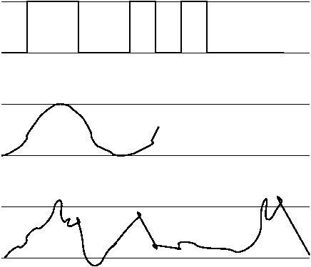
- Oscilloscope traces are shown on the right.
The vertical axis is voltage, the horizontal axis is time.
- Square wave—the ideal.
This is how we think of circuits.
The top figure.
- (Poorly drawn) Sine wave; middle figure.
- Actual wave; bottom figure.
- Non-zero rise times and fall times.
- Overshoots and undershoots.
- Glitches.
Not really quite as bad as the picture shows.
- A full engineering design must make sure to sample the signal
when it is stable.
Since this is not an engineering course, we will
ignore these issues and assume square waves.
In English, digit implies 10 (a digit is a finger), but not in
computers.
Indeed, the word Bit is short for Binary digIT and binary means
base 2 not 10.
0 and 1 are called complements of each other as are true and false
(also asserted/deasserted; also set/unset)
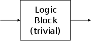
Logic Blocks: Combinational vs. Sequential
A logic block can be thought of as a black box that takes in
electrical signals and puts out other electrical signals.
There are two kinds of blocks.
- Combinational (or combinatorial)
- Does NOT have memory elements.
- Is much simpler than circuits with memory since the outputs
are a function of just the inputs and not any pre-existing
state.
That is, if the same inputs are presented on Monday and
Tuesday, the same outputs will result.
- Sequential
- Contains memory.
- The current value in the memory is called the state of the
block.
- The output depends on the input AND on the state.
- Consider reading a RAM.
There are two inputs: the memory address, and the operation
(read vs write).
- Certainly reading location 1011001 on Monday does not
necessarily give the same result as reading the same
location on Tuesday.
We shall study combinational blocks first and will will study
sequential blocks later (in a few lectures).
Truth Tables
Since combinatorial logic has no memory, it is simply a
(mathematical) function from its inputs to its outputs.
A common way to represent the function is using a
Truth Table.
A Truth Table has a column for each input and a
column for each output.
It has one row for each possible set of input values.
So, if there are A inputs, there are 2A rows.
In each of these rows the output columns have the output for that
input.
Such a table is possible only because there are only a finite
number of possible input values.
Consider trying to produce a table for the mathematical
function
y = f(x) = x3 + 6x2 - 12x - 3.5
There would be only two columns (one for x and one for
y) but there would need to be an infinite number of rows!
A Numbers Game—How Many Possible Truth Tables Are There?
1-input, 1-output Truth Tables
Let's start with a really simple truth table, one
corresponding to a logic block with one input and one output.
How many different truth tables are there for a
one input one output
logic block?
1-input, 1-output Truth Table
| In | Out |
|---|
| 0 | ? |
| 1 | ? |
There are two columns (1+1) and two rows (21).
Hence the truth table looks like the one on the right with the
question marks filled in.
Since there are two question marks and each one can have one of two
values there are just 22=4 possible truth tables.
They are:
- The constant function 1, which has output 1 (i.e., true) for either
input value.
- The constant function 0.
- The identity function, i.e., the function whose output equals
its input.
This logic block is sometimes called a buffer.
- An inverter.
This function has output the opposite of the input.
We will see symbols for the last two possibilities very soon.
2-input, 1-output Truth Table
| In1 | In2 | Out |
|---|
|
|
|
| 0 | 0 | ? |
| 0 | 1 | ? |
| 1 | 0 | ? |
| 1 | 1 | ? |
2-input, 1-output Truth Tables
Three columns (2+1) and 4 rows (22).
How many such truth tables are there?
It is just the number ways can you fill in the output entries,
i.e. the question marks.
There are 4 output entries so the answer is 24=16.
Larger Truth Tables
In general the number of question marks is the
number of rows times the number of output columns.
How about 2 in and 3 out?
- 2+3=5 columns (3 of them output columns, where the question
marks appear).
- 22=4 rows.
- 4*3=12 question marks.
- 212=4096 possibilities.
3 in and 7 out?
- 10 columns (7 of them output).
- 23=8 rows.
- 28*7 = 256 = 232*224
or about about 4 billion times 16 million possibilities.
- Question: How do I know 232 is about
4 billion and 224 is about 16 million?
Answer: I remember that
210=1024.
n in and k out?
- n+k columns (k are output).
- 2n rows.
- 22n*k possibilities.
This gets really big very fast!
Boolean Algebra
We use a notation that looks like algebra to express logic functions and
expressions involving them.
The notation is called Boolean algebra in honor of
George Boole.
A Boolean value is a 1 or a 0.
A Boolean variable takes on Boolean values.
A Boolean function takes in boolean variables and
produces boolean values.
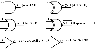
Four Boolean functions are especially common.
- The (inclusive) OR Boolean function of two variables.
Draw its truth table on the board.
This function is written + (e.g. X+Y where X and Y are Boolean
variables) and is often called the logical sum.
When we write 0 for false and 1 for true, three out of four output
values in the truth table are the same as the result for a normal
(mathematical) sum.
- AND.
Draw its truth table on the board.
AND is often called the logical product and written as a
centered dot (like the normal product in regular algebra).
So we would write A·B
for A AND B.
I sometimes write it as a period, because that is easier in
html.
As in regular algebra, when all the logical variables are just
one character long, we indicate the product by juxtaposition,
For example, when variables are each one character long,
AB represents the product of A
and B.
All four truth table values are the same for the logical product
as they are for the normal (mathematical) product.
- NOT.
Draw its truth table on the board.
This is a unary operator (i.e., it has only one argument, not two
as above; functions with two inputs are called binary
operators).
NOT A is written A with a bar over it
Ā, which is hard to do in html so I instead often
write A'.
- Exclusive OR (XOR).
Draw its truth table on the board.
XOR is written ⊕, a + with a circle around it.
A⊕B is True if exactly one input is
true.
In particular, note that 1⊕1 = 0.
Homework: Draw the
truth table of the Boolean function of 3 boolean variables that is
true if and only if exactly 1 of the 3 variables is
true.
Homework: What is the
cycle time of a 250MHz computer?
Some manipulation laws
Remember this is called Boolean Algebra.
- Identity (recall that I often use · for and):
- A+0 = 0+A = A
- A·1 = 1·A = A
- Inverse (recall that I use ' for not):
- A+A' = A'+A = 1 (NOT has the highest precedence)
- A·A' = A'·A = 0
- The name inverse is somewhat funny since
- If you Add the inverse you get the
identity for Product.
- If you Multiply by the inverse you get
the identity for Sum.
- Commutative Laws:
- A+B = B+A
- A·B = B·A
- Due to the commutative laws, we see that both the identity and
inverse laws contained redundancy.
For example, from A+0 = A and the commutative law we get that
0+A = A without stating the latter explicitly.
- Associative Laws:
- A+(B+C) = (A+B)+C
- A·(B·C)=(A·B)·C
- Due to the associative law we can write A·B·C without
parentheses since either order of evaluation gives the same
answer.
Similarly we can write A+B+C without parentheses.
- Distributive Laws:
- A·(B+C)=A·B+A·C
- Note also that like the situation for
ordinary algebra, multiplication has higher precedence than
addition if no parentheses are used.
- A+B·C=A+(B·C)=(A+B)·(A+C)
- Note that, unlike the situation for ordinary
algebra, both distributive laws are valid.
- DeMorgan's Laws:
- (A+B)' = A'B'
- (AB)' = A'+B'
How does one prove these laws?
Answer: It is simple, but tedious.
Write the truth tables for each side and see that the outputs are
the same.
You can write just one truth table with columns for all the inputs
and for the outputs of both sides.
You often write columns for intermediate outputs as well, but that
is only a convenience.
The key is that you have a column for the final value of the LHS
(left hand side) and a column for the final value of the RHS and
that these two columns have identical results.
Prove the first distributive law on the board.
The following columns are required: the inputs A, B, C; the LHS
A(B+C); and the RHS AB+AC.
Beginners like us would also use columns for the intermediate
results B+C, AB, and AC.
(Note that I am now indicating product by simple
juxtaposition.)
For practice do it three ways:
- Two truth tables each with all the variables as input columns.
One has the LHS as the output column.
The other has the same input columns but the RHS is the output
column.
- One truth table.
The input columns are the variables and there are two output
columns: the LHS and the RHS.
- The same as ii but with some intermediate result columns.
Start Lecture #2
Homework: 1 (A number
given with a problem refers to the problems in the book at the end
of the current chapter; I often write out the problem as well).
Prove DeMorgan's Laws (via truth tables).
The book has a defect.
It gives the solution with the problem.
Do it anyway.
Lab 1 Part 2:
Prove
the second distributive law via logisim.
Specifically produce a circuit (use the default name main) with
three inputs A, B, and C and 2 two outputs A+B·C and
(A+B)·(A+C).
The two outputs should have the same logical value for all possible
input values.
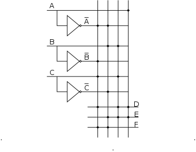
| A | B | C | D | E | F |
|---|
|
|
| 0 | 0 | 0 | 0 | 0 | 0 |
| 0 | 0 | 1 | 1 | 0 | 0 |
| 0 | 1 | 0 | 1 | 0 | 0 |
| 0 | 1 | 1 | 1 | 1 | 0 |
| 1 | 0 | 0 | 1 | 0 | 0 |
| 1 | 0 | 1 | 1 | 1 | 0 |
| 1 | 1 | 0 | 1 | 1 | 0 |
| 1 | 1 | 1 | 1 | 0 | 1 |
Let's do on the board the example on page B-5.
Consider a logic function with three inputs A, B, and C; and three
outputs D, E, and F defined as follows:
- D is true if at least one input is true.
- E is true if exactly two inputs are true.
- F is true if all three inputs are true.
The goal is to compute the truth table and the logic
equations.
Constructing the truth table is straightforward; simply fill in the
24 output entries by looking at the definitions of D, E, and F.
The result is shown on the right.
Producing the logic equations for D, E, and F can be done in
two ways.
- Examine the column of the truth table for a given output and
write one term for each entry that is a 1.
This method requires constructing the truth table and might be
called the method of perspiration.
- Look at the definition of D, E, and F and just
figure it out
.
This might be called the method of inspiration.
For D and F it is fairly clear.
E requires some cleverness: the key idea is that
exactly two are true
is the same as
(at least) two are true AND it is not the case that all
three are true
.
So we have the AND of two expressions: the first is a three
way OR and the second the negation of a three way AND.
The first way we produced the logic equation shows
that any logic equation can be written using just
AND, OR, and NOT.
Indeed it shows more.
Each entry in the output column of the truth table corresponds to
the AND of several literals (in this case three
literals, because there are three inputs).
A literal is either an input variable or the negation of
an input variable.
In mathematical logic such a formula is said to be in
disjunctive normal form
because it is the disjunction
(i.e., OR) of conjunctions (i.e., ANDs).
In computer architecture disjunctive normal form is often called
two levels of logic because it shows any such formula can
be computed by passing signals through only two logic functions,
AND and then OR (assuming we are given the inputs and their
complements).
- First compute all the ANDs.
There can be many, many of these, but they can all be computed at
once using many, many AND gates.
- Compute the required ORs of the ANDs computed in step 1.
There is only one OR for each output variable, but that OR can
have many inputs.
Remark: Demo logisim for this problem (the file
is ~/courses/arch/logisim-projects/HP-example-1.circ.)
With DM (DeMorgan's Laws) we can do quite a bit without resorting to
truth tables.
For example one can ...
Homework: Show that the
two expressions for E in the example above are equal.
Start to do the homework on the board.
Remark: You should ignore any references to Verilog in
the textbook.
Gates
Gates implement the basic logic functions, e.g., AND OR NOT XOR
Equivalence.
When drawing logic functions, we use the standard shapes shown to
the right.
Note that none of the figures is input-output symmetric.
That is, one can tell which lines are inputs and which are
outputs without resorting to arrowheads and without
the convention that inputs are on the left.
Sometimes the figure is rotated 90 or 180 degrees.
We show two inputs for AND, OR, and XOR.
It is easy to see that AND and OR make sense for more inputs as
well.
For XOR it is not so clear and not standardized.
Bubbles
We often don't draw inverters and draw instead
little circles at the input or output of the other gates (e.g., AND
OR).
These little circles are sometimes called bubbles.
This convention explains why the inverter is drawn as a buffer with
an output bubble.
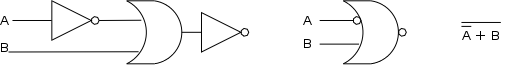
For example, the diagram on the right shows three
ways a writing the same logic function: using inverters, using
bubbles, or algebraically.
Show on the board that the picture above for equivalence is
correct. i.e., show that equivalence is the negation of XOR.
Specifically, show that AB + A'B' = (A ⊕ B)'.
  (A ⊕ B)' =
  (A'B+AB')' =
  (A'B)' (AB')' =
  (A''+B') (A'+B'') =
  (A + B') (A' + B) =
  (A + B') A'  +  (A + B') B =
  AA' + B'A' + AB + B'B =
  0   + B'A' + AB + 0 =
  AB + A'B'
Homework: 4.
Homework: Recall the
Boolean function E that is true if and only if exactly 2 of the
three variables is true.
You have already drawn the truth table.
Draw a logic diagram for E using AND OR NOT.
Draw a logic diagram for E using AND OR and bubbles.
Universal Gates
A set of gates is called universal if these gates are
sufficient to generate all logic functions.
- Since we have seen that any logic function can be written in
disjunctive normal form, all logic functions can be constructed
from AND, OR, and NOT.
So this triple is universal.
- Question: Are there any pairs that are
universal?
Answer: Sure, A+B = (A'B')' so we can
get OR from AND and NOT.
Hence the pair AND NOT is universal.
Similarly, we can get AND from OR
and NOT and hence the pair OR NOT
is universal.
- Could there possibly be a single function that is universal all by
itself?
AND won't work as you can't get NOT from
just AND
OR won't work as you can't
get NOT from just OR
NOT won't work as you can't get AND from
just NOT.
- But there indeed is a universal function!
In fact there are two of them.
Definition: NOR
(NOT OR) is true when OR is false.
Draw the truth table on the board.
Definition: NAND
(NOT AND) true when AND is false.
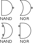
Draw the truth table on the board.
We can draw both NAND and NOR in two ways as
shown in the diagram on the right.
The top pictures are from the definition; the bottom use DeMorgan's
laws.
Theorem
A 2-input NOR is universal and
a 2-input NAND is universal.
Proof
We will show that you can get A', A+B, and AB using just a two
input NOR.
- A' = A NOR A
- A+B = (A NOR B)' (we can use ' by above)
- AB = (A'+B')'
Draw the truth tables showing the last three statements.
Also say why they are correct, i.e., we are now at the point
where simple identities like these don't need truth tables.
Question: Why would it have been enough to show
that you can get A' and A+B.
Answer: Because we already know that the
pair OR NOT is universal.
It would also have been enough to show that you can get A' and AB.
Lab 1 Part 3: A
2-input NAND is universal.
- Use logisim to draw a circuit for an inverter using
just NAND.
You can find NAND in
Gates
.
Name the circuit NOT.
- Use logisim to draw a circuit for AND using just
NAND and NOT.
You may use the built in inverter for NOT since you already showed
how to build NOT from NAND.
Name the circuit AND.
- Use logisim to draw a circuit for OR using just NAND
and NOT.
Name the circuit OR.
- Congratulate yourself for proving that NAND is universal!
- Save the file as univ.circ (it has three circuits).
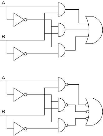
Sneaky way to see that NAND is universal.
- First show that you can get NOT from NAND as
we did above.
Hence we can use inverters and bubbles.
- Now imagine that you are asked to do a circuit for some function
with N inputs.
Assume you have only one output.
- Using inverters you can get 2N signals the N original and N
complemented.
- Recall that the natural sum of products form that we obtained
from the truth table.
Each term is an AND of some of the original and complemented
inputs; These terms feed into one (giant) OR.
- The top picture shows a small example, AB + A'B +A'B'.
In this example N=2 so we have 2 original inputs and 2
complemented inputs.
- Note that T intersections indicate
electrical connections; whereas, the crossings do not.
- If you want a crossing to indicate a connection, use a solid
dot.
- Naturally you can add a pair of bubbles to each end of a wire
since those bubbles will
cancel
.
- The bottom right picture shows the canceling bubbles added to
the picture above.
- But now all the gates are NANDS!!
- This argument shows universality providing you
permit giant NANDs, i.e.,
NANDS with arbitrary many inputs.
- To complete the proof you would show
that NAND(A,B,C) can be written with
just 2-input NANDs.
Minimizing the Gate Count
We have seen how to implement any logic function
given its truth table.
Indeed, the natural implementation from the truth table uses just
two levels of logic.
But that implementation might not be the simplest possible.
That is, we may have more gates than are necessary.
Minimizing the number of gates is decidedly NOT
trivial; we do not cover it in this course.
Some texts, including one by Mano that I used a number of years
ago, cover the topic of gate minimization in detail.
I actually like the topic, but it takes a few lectures to cover
well and it is no longer used in practice since it is done
automatically by CAD tools.
Minimization is not unique, i.e. there can be two or more minimal
forms.
Given A'BC + ABC + ABC'
Combine first two to get BC + ABC'
Combine last two to get A'BC + AB
Don't Cares (preview)
Sometimes when building a circuit, you don't care what the output
is for certain input values.
For example, that input combination might be known not to occur.
Another example occurs when, for some combination of input values, a
later part of the circuit will ignore an output of this part.
Both of these two are called don't care outputs.
Making use of don't cares can reduce the number of gates needed.
One can also have don't care inputs when, for
certain values of a subset of the inputs, the output is already
determined and you don't have to look at the remaining inputs.
We will see a case of this very soon when we do multiplexors.
An aside on theory
Putting a circuit in disjunctive normal form (i.e. two levels of
logic) means that every path from the input to the output goes
through very few gates.
In fact only two, an OR and an AND.
Maybe we should say three since the AND can have a NOT (bubble).
Theoreticians call this number (2 or 3 in our case) the
depth of the circuit.
Se we see that every logic function can be implemented with small
depth.
But what about the width, i.e., the number of gates.
The news is bad.
The parity function takes n inputs and gives TRUE
if and only if the number of TRUE inputs is odd.
If the depth is fixed (say limited to 3), the number of gates
needed for parity is exponential in n.
B.3 Combinational Logic
Decoders (and Encoders)
Imagine you are writing a program and have 32 flags, each of which
can be either true or false.
You could declare 32 variables, one per flag.
If permitted by the programming language, you would declare each
variable to be a bit.
In a language without bits you might use a single 32-bit int and
play with shifts and masks to store the 32 flags in this one
word.
In either case, an architect would say that you have these flags
fully decoded.
That is, you can specify the values of each of the bits.
Now imagine that for some reason you know that, at all
times, exactly one of the flags is true and the
other are all false.
Then, instead of storing 32 bits, you could store a 5-bit integer
that specifies which of the 32 flags is true.
This is called fully encoded.
For an example, consider radio buttons
on a web page.
A 5-to-32
decoder converts an encoded 5-bit signal into the
decoded 32-bit signal having the one specified signal true.
A 32-to-5
encoder does the reverse operations.
Note that the output of an encoder is defined
only if exactly one input bit is
set (recall set means true).
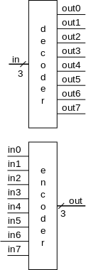
The the top diagram on the right shows a 3-to-8 decoder.
- Note the
3
with a slash, which signifies a three bit
input.
This notation represents a bundle of three (1-bit) wires, often
called a 3-bit line.
- I could have drawn the output wires the same way.
However, one normally uses the slash notation only if the entire
line travels together.
- A decoder with n input bits, produces 2n output
bits.
- View the input as
k written as an n-bit binary number
and view the output as 2n bits with the k-th bit set
and all the other bits clear.
- Implement the 3-to-8 decoder on the board with simple
gates.
Similarly, the bottom diagram shows an 8-3 encoder.
- Again the slash notation is used to indicate a multi-bit line
(i.e., a bundle of wires).
- Remember that the output of a encoder is defined
only if exactly one input is
set.
Why do we use decoders and encoders?
- The encoded form takes (MANY) fewer bits so is better for
communication.
- The decoded form is easier to work with in hardware since
there is no direct way to test if 3 wires represent a 5
(101).
You would have to test each wire.
But it easy to see if the encoded form is a five; just test
the fifth wire, out5.
Lab 1 Part 4:
- (15 points) Use logisim to draw a circuit for a 2-to-4 decoder
using just AND/OR/NOT (NOT is called an inverter).
Save this circuit as 2-4.circ.
- (15 points) Use logisim to draw a circuit for a 4-to-2 encoder
using just AND/OR/NOT.
Save this circuit as 4-2.circ
- (5 points) Connect the four outputs of the decoder to the
corresponding 4 inputs of the encoder.
The resulting logisim circuit has two inputs and two outputs.
It should be the identity.
Save this circuit as 2-2-id.circ.
Lab 1 is assigned and
is due in one week.
The official version of all labs are on nyu classes As mentioned
previously, the versions in these notes are fairly close
approximations.
Start Lecture #3
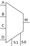
Multiplexors
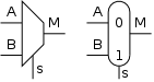
A multiplexor, often called a mux or
a selector is used to select one (output) signal
from a group of (input) signals based on the value of a group of
(select) signals.
In the 2-input mux shown on the right, the select line S is thought of
as an integer 0..1.
If the integer has value j then the jth input is sent to
the output.
Construct on the board an equivalent circuit made from ANDs and ORs
(and bubbles) in two ways:
- Construct a truth table with 8 rows (don't forget that,
despite its name, the select line is an input) and write the sum
of product form, one product for each row and a large 8-input
OR.
This is the canonical two-levels of logic solution.
(Method of perspiration.)
- A simpler, more clever, two-levels of logic solution.
Two ANDs, one per input (not including the selector).
The selector goes to each AND, one with a bubble.
The output from the two ANDs goes to a 2-input OR.
(Method of inspiration.)
The diagram on the right shows a 4-input MUX.
Construct on the board an equivalent circuit with ANDs and ORs in
three ways:
- Construct the truth table (64 rows!) and write the sum of
products form.
This form has one product (a 6-input AND) for each row where the
output is 1 and
a gigantic OR of all these products.
Just start this, don't finish it.
(Perspiration.)
- A simpler, more clever, two-level logic solution.
Four ANDS (one per input), each gets one of the inputs and both
select lines with appropriate bubbles.
The four outputs go into a 4-way OR.
(Inspiration.)
- Construct a 2-input mux (using the clever solution).
Then construct a 4-input mux using a tree of three 2-input
muxes.
One select line is used for the two muxes at the base of the
tree, the other is used at the root.
(Hierarchical.)
This last solution is our first illustration of the usefulness of
the hierarchical feature of logisim.
All three of these methods generalize to a mux with 2k
input lines, and k select lines.
A 2-way mux is the hardware analogue of if-then-else.
    if S=0
        M=A
    else
        M=B
    endif
A 4-way mux is an if-then-elif-elif-else
    if S1=0 and S2=0
        M=A
    elif S1=0 and S2=1
        M=B
    elif S1=1 and S2=0
        M=C
    else      // S1=1 and S2=1
        M=D
    endif
Don't Cares (again)
| S | In0 | In1 | Out |
|---|
|
|
| 0 | 0 | X | 0 |
| 0 | 1 | X | 1 |
| 1 | X | 0 | 0 |
| 1 | X | 1 | 1 |
Consider a 2-input mux.
If the selector is 0, the output is In0 and the value of In1 is
irrelevant.
Thus, when the selector is 0, In1 is a don't care input.
Similarly, when the selector is 1, In0 is a don't care input.
On the right we see the resulting truth table.
Recall that without using don't cares the table would have 8 rows
since there are three inputs; in this example the use of don't cares
reduced the table size by a factor of 2.
The truth table for a 4-input mux has 64 rows, but the use of don't
care inputs has a dramatic effect.
When the selector is 01 (i.e., S1 is 0 and S0 is 1), the output
equals the value of In1 and the other three In's are don't care.
A corresponding result occurs for other values of the selector.
The above are don't care inputs.
Recall that a don't care output occurs when for some input values
(i.e., rows in the truth table), we don't care what the value is for
certain outputs.
- Perhaps we know that this set of input values is impossible.
- Perhaps we know that we will
mux out
these outputs when
we have the specified inputs.
Homework: Draw the
truth table for a 4-input mux making use of don't care inputs.
What size reduction occurred with the don't cares?
Homework: B.13.
B.10. (Assume you have constant signals 1 and 0 as well.)
Powers of 2 NOT Required
How can one construct a 5-way mux?
Construct an 8-way mux and use it as follows.
- Connect the five input signals to the first five inputs of the
mux.
- Make sure the three select inputs never result in 5, 6, or 7.
Can do better by realizing the select lines equaling 5, 6, or 7
are don't cares and hence the 5-way can be customized and would use
fewer gates than an 8-way mux.
Lab 2 Part 1 Muxes:
Reread the section in the notes on multiplexors and use logisim to
redo some of what I did in class.
- Construct a 2-input (1-bit-wide) mux using the
simpler, more clever, two-levels of logic solution
.
Name this circuit mux-2.
- Construct a 4-input (1-bit-wide) mux two ways.
- Using four ANDs (one per input) and a 4-input OR.
Name this circuit mux-4i.
- Using three of the mux-2 circuits you constructed earlier in
the lab.
Name this circuit mux-4ii.
Use logisim's subcircuit feature, i.e., use the
load library
entry of the circuit tab.
Two Level Logic and PLAs (and PALs)
| A | B | C | D | E | F |
|---|
|
|
| 0 | 0 | 0 | 0 | 0 | 0 |
| 0 | 0 | 1 | 1 | 0 | 0 |
| 0 | 1 | 0 | 1 | 0 | 0 |
| 0 | 1 | 1 | 1 | 1 | 0 |
| 1 | 0 | 0 | 1 | 0 | 0 |
| 1 | 0 | 1 | 1 | 1 | 0 |
| 1 | 1 | 0 | 1 | 1 | 0 |
| 1 | 1 | 1 | 1 | 0 | 1 |
The idea behind PLAs (Programmable Logic Arrays) is to partially
automate the algorithmic way you can produce a circuit diagram in
the sums of product form from a given truth table.
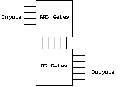
Since the form of the circuit is always a bunch of ANDs feeding into
a bunch of ORs, we can manufacture
all the gates in advance
of knowing the desired logic functions and, when the functions are
specified, we just need to make the necessary connections from the
ANDs to the ORs.
In essence all possible connections are configured but with switches
that can be open or closed.
Actually, the words above better describe a PAL (Programmable Array
Logic) than a PLA, as we shall soon see.
Consider the truth table on the upper right, which we have seen
before.
It has three inputs A, B, and C, and three outputs D, E, F.
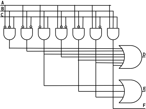
Below it we see the corresponding logic diagram in sum of products
form.
Recall how we construct this diagram from the truth table.
- There is one AND for each
relevant
row.
- There is a big OR for each output.
The OR has one input for each row that the output is true.
But
- If a row does not contribute to any output (e.g., the first
row of this truth table), then it is an
irrelevant
row
and there is no AND.
- If an output is true for only one row (e.g. F in this
truth table), then we omit the OR with one input, which
would be just a buffer (i.e., the identity function).
- If an output is true for no row (there is no such output
in this example), then the output is always FALSE.
I guess this could be drawn as an OR with no inputs, but I
have never seen it drawn that way.
Instead, it would be drawn as a constant 0.
- If an output is true for all rows (there is no such output
in this example), then the output is always TRUE.
I guess this could be drawn as an AND with no inputs, but I
have never seen it drawn that way.
Instead, it would be drawn as a constant 1.
- Since there are 7 rows for which at least one output is true,
there are 7 product terms that will be used in one or more of
the ORs (in fact all seven will be used in D, but that is
special to this example).
- Each of these product terms is called a Minterm.
- So we need seven ANDs, one for each minterm.
Each AND takes a subset of A, B, C, A', B', and C' as inputs.
In fact we can say more since some subsets (e.g., A and A') are
never used.
Instead of arbitrary subsets of the 6 inputs, we choose three
inputs, either A or A', either B or B', and either C or C'.
However, we will not make use of this refinement in the next
diagram.
- This collection of ANDs is called the
AND plane and the collection of ORs mentioned
above is called the OR plane.
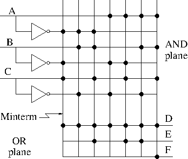
The reason for calling them planes is clearer in the second
diagram, which shows the same information in a more schematic
style.
- This third figure shows more clearly the AND plane, the OR
plane, and the minterms.
- Rather than having bubbles (i.e., custom AND gates that invert
certain inputs), we
simply invert each input once and send the inverted signal all the way
accross.
- AND gates are shown as vertical lines; ORs as horizontal.
- Note the dots used to represent connections.
- Notice that all PLAs with N inputs and M
outputs look the same geometrically.
The only difference between two different (N,M) PLAs is
where to put the dots (connections).
- When a PLA is manufactured all the specified connections are
made.
That is, a manufactured PLA is specific for a given circuit.
Hence the name Programmable Logic Array is
somewhat of a misnomer since the device is not
programmable by the user.
- Imagine instead building a bunch of these templates but not yet
specifying where the dots go.
This is called a PAL (Programmable Array Logic), and is discuss
next.
- Finally, we can draw a PLA in the even more abstract form shown
on bottom right.
Homework: Consider a
logic function with three inputs and two outputs.
The first output is true if one or two of the inputs are true and
the second output is true if one or three inputs are true.
Draw a PLA for this circuit.
PAL (Programmable Array Logic)
A PAL can be thought of as a PLA in which the final dots are made
by the user.
The manufacturer produces a sea of gates
.
The user programs it to the desired logic function by adding the
dots.
ROMs
One way to implement a Java function without side effects is to
perform a table lookup.
A ROM (Read Only Memory) is the analogous way to implement a logic
function.
- A math function f is given x and produces f(x).
- A ROM is given an address and produces the value stored at
that address.
- Normally math functions are defined for an infinite number of
values, for example f(x)=3x for all real numbers x.
- We can't build an infinite ROM (sorry), so we are only
interested in functions defined for a finite number of values.
Today a billion is OK, but a trillion is too big.
- How do we create a ROM for the function f(3)=4, f(6)=20 all other
values don't care?
Simply purchase a ROM with 4 in address 3 and 20 in address 6.
- Consider a function defined for all n-bit numbers (say n=20) and
having a k-bit output for each input.
- View an n-bit input as n 1-bit inputs.
- View a k-bit output as k 1-bit outputs.
- Since there are 2n possible inputs and each
requires a k 1-bit output, there are a total of
(2n)k possible bits of output, i.e. the ROM must
hold (2n)k bits.
- Now consider a truth table with n inputs and k outputs.
The total number of output bits is again (2n)k
(2n rows and k output columns).
- Indeed a ROM implements a truth table, i.e. it is a logic
function.
Important: A ROM does not have state.
It is another combinational circuit.
That is, we do not consider a ROM as memory
.
The reason is that once a ROM is manufactured, the output depends
only on the input.
I realize this sounds wrong, but it is right.
Indeed, we will shortly see that a ROM is like a PLA.
Both are structures that can be used to implement a truth table.
The key property of combinational circuits is that the outputs
depend only on the inputs.
This property (having no state) is false for a RAM chip: The input
to a RAM is (like the input to a ROM) an address and (unlike a ROM)
an operation (read vs. write).
The RAM (given a read request) responds by presenting at its outputs
the value CURRENTLY stored at that address.
Thus knowing just the input (i.e., the address and the operation) is
NOT sufficient for determining the output.
Whereas; knowing the address supplied to a given
ROM IS sufficient to determine the output.
A PROM is a programmable ROM.
That is, you buy the ROM with nothing
in its memory and
then before it is placed in the circuit you load the
memory, and never change it.
This is like a CD-R.
Again, as with a ROM, when you are using a PROM in a circuit, the
output is determined by the input (the address) and hence a PROM is
another combinatorial circuit.
An EPROM is an erasable PROM.
It costs more but if you decide to change its memory this is
possible (but is slow).
This is like a CD-RW.
Normal
EPROMs are erased by some ultraviolet light process
that is performed outside the circuit.
But EEPROMs (electrically erasable PROMS) are
not as slow and are done electronically.
Since this is done inside the circuit you could consider it a RAM if
you considered the erasing as a normal circuit operation.
Flash is a modern EEPROM that is reasonably
fast.
Most of these EPROMS are erasable not writable, i.e. you can't just
change one byte to an arbitrary value.
(Modern flash can nearly replace true RAM and perhaps should not be
called EPROMS).
ROMs and PLAs
A ROM is similar to PLA
- Both can, in principle, implement any truth table.
- Neither is (user) programmable.
- A 2Mx8 ROM really implement any truth table with 21 inputs
(221=2M) and 8 outputs.
- It stores 2M bytes.
- In ROM-speak, it has 21 address pins and 8 data pins.
- A PLA with 21 inputs and 8 outputs might need to have 2M minterms
(AND gates).
- The number of minterms depends on the truth table itself.
- For normal truth tables with 21 inputs the number of
minterms is much less than 221.
- The PLA is manufactured with the number of minterms needed.
A PROM is similar to a PAL.
- Both can, in principle, implement any truth table.
- Both are user programmable.
- A PROM with n inputs and k outputs can implement any truth
table with n inputs and k outputs.
- An n-input, k-output PAL that you buy does not have enough
gates for all possibilities since most truth tables with n
inputs and k outputs require far fewer than 2nk
gates.
Don't Cares (Bigger Example)
Sometimes not all the input and output entries in a truth table are
needed.
We indicate this with an X and it can result in a smaller truth
table.
There are two classes of don't cares: input don't cares and output
don't cares.
All this was mentioned before.
Now that we are more experienced with truth tables and their logic
diagrams, we can consider a larger example.
Full Truth Table
| A | B | C | D | E | F |
|---|
|
|
| 0 | 0 | 0 | 0 | 0 | 0 |
| 0 | 0 | 1 | 1 | 0 | 1 |
| 0 | 1 | 0 | 0 | 1 | 1 |
| 0 | 1 | 1 | 1 | 1 | 0 |
| 1 | 0 | 0 | 1 | 1 | 1 |
| 1 | 0 | 1 | 1 | 1 | 0 |
| 1 | 1 | 0 | 1 | 1 | 0 |
| 1 | 1 | 1 | 1 | 1 | 0 |
Truth Table with Output Don't Cares
| A | B | C | D | E | F |
|---|
|
|
| 0 | 0 | 0 | 0 | 0 | 0 |
| 0 | 0 | 1 | 1 | 0 | 1 |
| 0 | 1 | 0 | 0 | 1 | 1 |
| 0 | 1 | 1 | 1 | 1 | X |
| 1 | 0 | 0 | 1 | 1 | X |
| 1 | 0 | 1 | 1 | 1 | X |
| 1 | 1 | 0 | 1 | 1 | X |
| 1 | 1 | 1 | 1 | 1 | X |
Truth Table with Input and Output Don't Cares
| A | B | C | D | E | F |
|---|
|
|
| 0 | 0 | 0 | 0 | 0 | 0 |
| 0 | 0 | 1 | 1 | 0 | 1 |
| 0 | 1 | 0 | 0 | 1 | 1 |
| X | 1 | 1 | 1 | 1 | X |
| 1 | X | X | 1 | 1 | X |
Input Don't Cares
These don't cares occur when the output doesn't depend
on all the inputs.
More precisely, for certain values of a subset of the inputs, the
outputs are already determined and hence in this case the values of
the remaining inputs are irrelevant.
We saw this when we did muxes.
Consider the simplest case of a 1-bit wide, 2-way mux.
If the select line is zero, the value of the bottom input has no
effect on the output.
Hence for those rows of the truth table we do not need to know
the value of the bottom input, we in effect don't care
about that input.
A larger example is shown on the right and discussed just below.
Output Don't Cares
This occurs when, for certain values of the inputs, either value
of the output is OK.
- Maybe, other parts of the circuit make it clear that certain
input combinations are impossible.
- Maybe, for this input combination, the given output is not
used (perhaps it is
muxed out
downstream).
The Example
The top diagram on the right is the full truth table for the
following example (from the book).
Consider a logic function with three inputs A, B, and C, and three
outputs D, E, and F.
- If A or C is true, then D is true (independent of B).
- If A or B is true, then E is true (independent of C).
- F is true if exactly one of the inputs is true,
but we
don't care about the value of F if both D and E are true.
The full truth table has 7 minterms (rows with at least one nonzero
output).
The middle truth table has the output don't cares indicated.
Now we do the input don't cares
- B=C=1 ==> D=E=11 ==> F=X ==> A=X
- A=1 ==> D=E=11 ==> F=X ==> B=C=X
The resulting truth table is also shown on the right.
Below the third truth table, we see the corresponding PLA.
It has been significantly reduced in size by the don't cares.
Note that there are only four AND gates (corresponding to the four
minterms).
Indeed, only three are minterms non-trivial: The last row of the
truth table, which corresponds to the rightmost vertical line of the
diagram, is simply A and hence this vertical like does not need an
AND gate.
As mentioned previously, there are various techniques for minimizing
logic (see a book by Mano), but we will not cover them.
Arrays of Logic Elements
Often we want to consider signals that are wider than a single bit.
An array of logic elements is used when each of the individual bits
is treated similarly.
As we will soon see, sometimes most of the bits are treated
similarly, but there are a few exceptions.
For example, a 32-bit structure might treat the lob (low order bit)
and hob differently from the others.
In such a case we would have an array 30 bits wide and two 1-bit
structures.
Buses
A Bus is a collection of (say n) data lines
treated as a single logical (n-bit) value.
- We typically use an array of logic elements to process a bus.
- For example, the mux shown on the near right switches between
two 32-bit buses.
- We often indicate a bus in drawings by using thicker lines and
employing the
by n
notation.
- The diagram on the far right shows how to implement the 32-bit,
2-way mux by using thirty-two 1-bit, 2-way muxes.
Lab 2 Part 1 Muxes
(continued):
- Construct a 2-input, 6-bit-wide mux using the
simpler, more clever solution
from the notes.
Name the project mux-2-6.
We would call the result an array of logic elements.
Use the bit width, splitter, and wire bundle features from
logisim.
Note that the select line is NOT 6-bits wide
(that would be 6 independent select lines and would be used for a
64-input mux).
Instead the single 1-bit select line is broadcast to 6 places
(each place having 2 ANDs).
- Save the file as lab2-part1.circ.
B.4: Using a Hardware Description Language
B.5: Constructing a Basic Arithmetic Logic Unit (ALU)
We will produce logic designs for the integer
portion of the MIPS ALU.
The floating point operations are more complicated and will not be
implemented.
MIPS is a computer architecture used in embedded designs.
In the 80s and early 90s, it was quite popular for desktop (or
desk-side) computers.
This was the era of the killer micros
that decimated the
market for minicomputers.
(When I got a DECstation desktop with a MIPS R3000, I think that,
for a short while, it was the fastest integer
computer at NYU.)
Much of the design we will present (indeed, all of the beginning
part) is generic.
I will point out when we are tailoring it for MIPS.
Homework
- Add the following pairs of 5-bit (unsigned) numbers.
The result might be a 6-bit number.
Recall that base ordinary base 10 addition does this as well
66666 + 55001 = 121667.
- 00111 + 10101
- 11111 + 00001
- 11111 + 11111
- How many cycles does a 5MHz computer execute in the time it
takes a 10MHz computer to execute 4 cycles.
Start Lecture #4
A 1-bit ALU
Our first goal will be a 1-bit wide structure that computes the
AND, OR, and SUM of two 1-bit quantities.
For the sum there is actually a third input, CarryIn, and a 2nd
output, CarryOut.
Since out basic logic toolkit already includes AND and OR gates,
our first real task is a 1-bit adder.
Half Adder
If the overall objective was a 1-bit ALU, then we would not have a
CarryIn.
However, we will be constructing a 32-bit ALU and, for a multi-bit
ALU, the CarryIn for each bit (other than the low order bit LOB) is
the CarryOut of the preceding lower-order bit.
We will number the bits from right to left so that the LOB is bit
number 0 and the HOB is bit number 31 (some, but not all computers
do this).
With this convention the CarryIn to bit number 4 (normally called
bit 4) is the CarryOut from bit 3.
When we don't have a CarryIn, the structure is sometimes called
a half adder
.
Don't treat the name too seriously; it is not half of an adder and
does not produce (A+B)/2.
A half adder has the following inputs and outputs.
- Two 1-bit inputs: X and Y.
- Two 1-bit outputs S (sum) and Co (carry out).
- No carry in.
Draw the truth table on the board.
Homework: Draw the
logic diagram for this half adder.
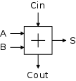
Full Adder
The full adder includes the carry-in.
The symbol a full adder is shown on the right
- Three 1-bit inputs: X, Y and Ci.
- Two 1-bit output: S and Co.
- S =
the total number of 1s in X, Y, and Ci is odd
- Co = #1s is at least 2.
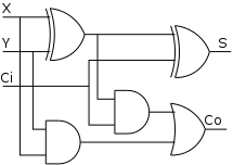
Below the symbol for the full adder is a logic diagram for it.
This diagram uses logic formulas for S and Co equivalent to the
definitions given above (see homework just below).
Homework
- Draw the truth table for a 1-bit full adder (8 rows).
- Show S = X ⊕ Y ⊕ Ci.
- Show Co = XY + (X ⊕ Y).Ci
Lab 2 Part 2i: Use
logisim to produce a 1-bit full adder.
This circuit has three 1-bit inputs and two 1-bit outputs.
Name the circuit fa-1.
Combining 1-bit AND, OR, and ADD
We have implemented 1-bit versions of AND (a basic gate), OR (a
basic gate), and SUM (the full adder just constructed).
Our next goal is a single structure that given two 1-bit inputs A
and B, can produce either A AND B, A OR B, or A + B.
We introduce another input named operation, a so
called control line
, to indicate which of the three
possibilities is desired.
There is a general principle used to produce a structure that
yields either X or Y depending on the value
of operation.
- Implement a structure that always computes X.
- Implement another structure that always
computes Y.
- Mux X and Y together
using operation as the select line.
This mux, with an operation select line, gives a
structure that sometimes
produces one result
and sometimes
produces another.
Note that internally both results
are always produced.
In our case we have three possible results so we need a 3-way mux
and the select line is a 2-bit wide bus.
With a 2-bit select line we can actually specify 4 operations; for
now we are using only three.
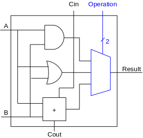
We show the diagram for this 1-bit ALU on the right.
In subsequent diagrams the Operation
input will be shown in
green to distinguish it as a control line rather than a data line.
(Now is it drawn in blue to show that it is introduced in this
diagram.)
The goal is to produce two bits of result from 2 (AND, OR) or 3
(ADD) bits of data.
The 2 bits of control tell what to do, rather than what data to do
it to.
The extra data output (CarryOut) is always produced.
Presumably if the operation is AND or OR, CarryOut is not used.
It is an example of a don't care
output.
Note: I believe the distinction between data and
control will become quite clear as we encounter more examples.
However, I wouldn't want to be challenged to give a (mathematically
precise) definition.
Lab 2 Part 2ii:
Use logisim to implement a 1-bit ALU that can perform, AND, OR, and
ADD of 1-bit quantities.
The circuit diagram is to the right.
Use a mux-4i from part 1 as your 3-input multiplexor (a logisim
subcircuit).
Use AND and OR basic gates.
Use fa-1 from part 2i as the adder (another logisim subcircuit).
Name the circuit alu-1.
Save the file containing both circuits for part2 (fa-1 and alu-1) as
lab2-part2.circ
A 32-bit ALU
A 1-bit ALU is interesting, but we need a 32-bit ALU to implement
the MIPS 32-bit operations, acting on 32-bit data values.
For AND and OR, there is almost nothing to do; a 32-bit AND is just
32 1-bit ANDs so we can simply use an array of logic elements.
However, ADD is a little more interesting since the bits are not
quite independent:
The CarryOut of one bit becomes the CarryIn of the next.
A 32-bit Adder
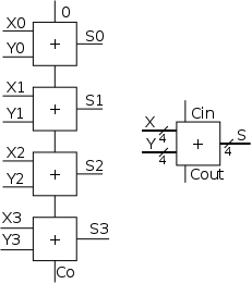
Let's start with a 4-bit adder.
- In the diagram to the near right, each box is a
1-bit full adder as above.
- The top FA is the low order bit (lob); the bottom FA is the hob.
- Note that the Carry-out of one 1-bit FA becomes the Carry-in
of the next higher order 1-Bit FA.
- Note also that you do the same thing when you add ordinary
(i.e., decimal) numbers.
- Further to the right we show the 4-bit adder without showing
the individual FAs.
- In this rightmost picture we have two 4-bit inputs (the
addends), one 1-bit input (the Carry-in), one 4-bit output (the
sum), and one 1-bit output (the Carry-out).
- If all you ever wanted from the rightmost circuit was 4-bit
addition, you would not have a Ci.
Instead you would feed zero into the Ci of the lob as I did in
the left picture.
- An advantage of the right diagram is that you can put two of
these 4-bit adders together to get an 8-bit adder.
Simply connect the Co of one to the Ci of the second.
How about a 32-bit adder, or even an an n-bit adder?
- No problem; just use n 1-bit FAs.
- Linear (time) complexity, i.e. the time for a 64-bit add is
(just about) twice that for a 32-bit add, which itself is (just
about) twice the time for a 16-bit add.
- This adder design is called ripple carry since the carry
ripples down the circuit from the low order bit to the high
order bit.
The necessity for the carry to ripple down the circuit one bit
at a time is why the circuit has linear complexity.
- Faster (logarithmic complexity) methods exist.
Indeed we will learn one soon.
Lab 2 Part 3: Use
logisim to implement a 4-bit full adder using four of the 1-bit full
adders as logisim sub-circuits.
The 4-bit full adder has two 4-bit inputs, one 1-bit input, one
4-bit output, and one 1-bit output.
Save the full circuit as lab2-part3.circ.
Lab 2 is now complete.
It is due in one week.
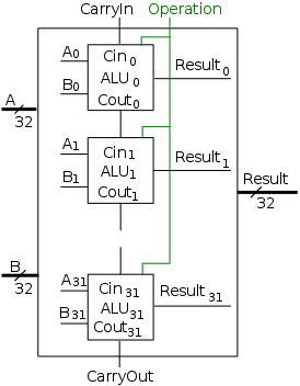
Combining 32-bit AND, OR, and ADD
To obtain a 32-bit ALU, we put together the 1-bit ALUs in a manner
similar to the way we constructed a 32-bit adder from 32 FAs.
Specifically we proceed as follows and as shown in the figure on the
right.
- Use an array of logic elements for the logic.
The individual logic element is the 1-bit ALU.
- Use buses for A, B, and Result.
In logisim terminology this means use splitters.
Broadcast
Operation to all
of the internal 1-bit ALUs.
This means wire the
external Operation to the
Operation input of each of the internal 1-bit ALUs.
This does not suggest a logisim splitter.- Wire the (overall) CarryIn to Cin for the lob.
- Wire Cout from the hob to the CarryOut
Facts Concerning (4-bit) Two's Complement Arithmetic
Note:
This is one place were the our treatment must deviate from the
book's.
Appendix B in the book assumes you have read the chapter on computer
arithmetic; in particular appendix B assumes that you know about
two's complement arithmetic.
I do not assume you know this material (although I suspect some of
you do).
I hear it was covered briefly in 201 and we will review it
later, when we do the arithmetic chapter.
What I will do here is assert some facts about two's complement
arithmetic that we will use to implement the circuit for SUB.
End of Note.
For simplicity I will be presenting 4-bit arithmetic.
We are really interested in 32-bit arithmetic, but the idea is the
same and the 4-bit examples are much shorter (and hence less likely
to contain typos).
4-bit Twos's Complement Numbers
With 4 bits, there are 16 possible numbers.
Since twos complement notation has one representation for each
number, there are 15 nonzero values.
Since there are an odd number of nonzero values, there
cannot be the same number of positive and negative
values.
In fact 4-bit two's complement notation has 8 negative values
(-8..-1), and 7 positive values (1..7).
(In one's complement notation there are the same number of positive
and negative values, but there are two representations for zero,
which is inconvenient.)
The high order bit (hob) on the left is the sign bit.
The sign bit is zero for positive numbers and for the number zero;
the sign bit is one for negative numbers.
Zero is written simply 0000.
1-7 are written 0001, 0010, 0011, 0100, 0101, 0110, 0111.
That is, you set the sign bit to zero and write 1-7 using the
remaining three lob's.
This last statement is also true for zero.
-1, -2, ..., -7 are written by taking the two's complement
of the corresponding positive number.
The two's complement is computed in two steps.
- Take the (ordinary) complement, i.e. change ones to zeros and
zeros to ones.
This is sometimes called the one's complement.
For example, the (4-bit) one's complement of 3 is 1100.
- Add 1.
For example, the (4-bit) two's complement of 3 is 1101.
If you take the two's complement of -1, -2, ..., -7, you get back
the corresponding positive number.
Try it.
If you take the two's complement of zero you get zero.
Try it.
What about the 8th negative number?
-8 is written 1000.
But if you take its (4-bit) two's complement, you
must get the wrong number because the correct
number (+8) cannot be expressed in 4-bit two's complement
notation.
Two's Complement Addition and Subtraction
Amazingly easy (if you ignore overflows).
- Add: Just use a 4-bit adder, do NOT treat the
sign bit in a special way, and discard the final carry-out.
- Sub: Take the two's complement of the subtrahend (the second
number) and add as above.
Implementing SUB (Together With AND, OR, and ADD)
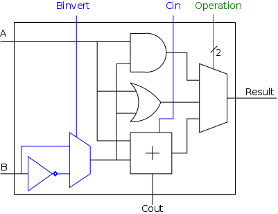
No change is needed to our circuit above to handle two's complement
numbers for AND/OR/ADD.
That statement is not clear for ADD and will be shown true later in
the course.
We wish to augment the ALU so that we can perform subtraction as
well.
As we stated above, A-B is obtained by taking the two's complement
of B and adding 1.
A 1-bit implementation is drawn on the right with the new structures
in blue (I often use blue for this purpose).
The enhancement consists of
- Using an inverter to get the one's complement of B.
- Using a mux with control
line Binvert
(in blue because it is new but
in green afterwards) to select
whether B or B' is fed to the adder.
- Using a clever trick to obtain the effect of adding B's two
complement when we are actually adding B's one complement.
Namely we set Cin, the carry-in to the lob, equal to 1
instead of 0.
This trick increases the sum by one and, as a result, calculates
(A+B')+1=A+(B'+1), which is A plus the two's complement of B,
which is A-B.
- As before, setting Operation to 00 and 01 gives AND
and OR respectively, providing we de-assert Binvert.
CarryIn is a don't care for AND and OR.
- To implement addition we use opcode 10 as before and de-assert
both Binvert and CarryIn
- To implement subtraction we again use opcode 10 but we assert
both Binvert and CarryIn
Lab 3 Part 1 Enhance
the 1-bit ALU from lab 2 to include subtraction as indicated
above.
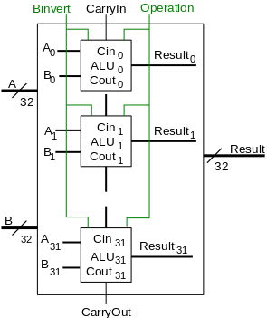
Extending to 32 Bits
A 32-bit version is simply a bunch of the 1-bit
structures wired together as shown on the right.
I use CarryIn and CarryOut when referring to
the external carry signals of the entire 32-bit structure.
Please do not confuse them with Cin and Cout,
the corresponding signals to each individual 1-bit structure.
- CarryIn is wired to Cin of the LOB and
Cout of the HOB is wired to CarryOut.
- The Binvert and Operation control lines are
broadcast to all of the 1-bit ALUs.
- As before Operation is 00 for AND, 01 for OR, and
10 for both ADD and SUB.
- For AND and OR de-assert BInvert.
CarryIn is a don't care.
- For addition de-assert both Binvert
and CarryIn.
- For subtraction assert both Binvert
and CarryIn.
- We could implement other functions as well.
For example, we get AB' by asserting Binvert and
setting Operation=00.
That one is not so useful, but a variant is useful and we will
implement it soon.
Tailoring the 32-bit ALU to MIPS
AND, OR, ADD, and SUB are found in nearly all ALUs.
In that sense, the construction up to this point has been generic.
However, most real architectures have some extras.
For MIPS they include.
- NOR, not very special and very easy.
- Overflow handling, common but not so easy.
Set on less than
(slt), not common and not so easy.- Equality test, not very special and easy.
Implementing NOR
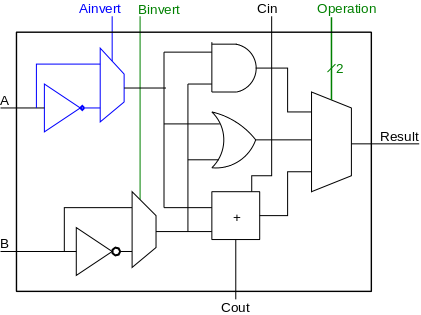
We noted above that our ALU already gives us the ability to
calculate AB', an uncommon logic function.
A MIPS ALU needs NOR and, by DeMorgan's law
A NOR B = (A + B)' = A'B'
which is rather close to AB', we need just invert A as
well as B.
The diagram on the right shows the added structures: an inverter
to get A', a mux to choose between A and A', and a control line for
the mux.
NOR is obtained by asserting Ainvert
and Binvert and setting Operation=00.
The other operations are done as before, with Ainvert
de-asserted.
The 32-bit version is straightforward.
All the bits are the diagram on the right.
Homework: Draw the
32-bit ALU that supports AND, OR, ADD, SUB, and NOR.
Overflows
Note: As with two's complement arithmetic, I
just present the bare boned facts here; they are
explained later in the course.
The facts are trivial (although the explanation is not).
Indeed there is just one fact.
- An overflow occurs for two's complement addition (which
includes subtraction) if and only if the carry-in to the sign
bit does not equal the carry out from the sign
bit.
Do on the board 4-bit twos complement addition of
- 1 + 1
- -1 + -1
Note that there is NO overflow despite a carry-out.
- 6 + 6
- -6 + -6
- -6 + 6
Start Lecture #5
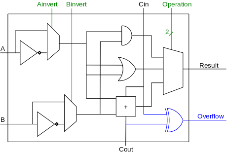
Only the hob portion of the ALU needs to be changed.
We need to see if the carry-in is not equal to the carry-out, but
not equal to
is exactly XOR.
The simple modification to the hob structure is shown on the right.
Homework: Draw the
32-bit ALU that supports AND, OR, ADD, SUB, and NOR and that asserts
an overflow line when appropriate.
Note that to ease the homework and, more importantly, the real
design, we can use the enhanced 1-bit ALU for all bits and simply
ignore the overflow output for all but the HOB.
Implementing Set on Less Than (SLT)
Definition of SLT
We are given two 32-bit, two's complement numbers A
and B as input and seek a 32-bit result that is 1 if A<B and 0
otherwise.
Note that only the lob of the result varies; the other 31 bits are
always 0.
The implementation is fairly clever as we shall see.
Idea #1
The first idea is simple.
The sign of A-B is 1 precisely
when A<B.
Thus, to implement slt, we need to set the LOB of the
result equal to the sign bit of the subtraction A-B, and set the
rest of the result bits to zero.
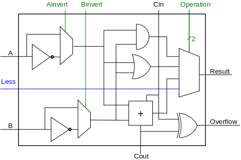
Idea #2
Give the 4-way mux another (i.e., a fourth) input,
called
Less.
This input is brought in from outside the bit cell.
To generate slt, we make the select line to the mux equal to 11 so
that the the output is the this new input.
See the diagram on the right.
- For all the bits except the LOB, the Less input is
zero.
This is trivial to do: Simply label a wire false
or 0, or de-asserted and connected it to the
31 Less inputs (i.e., all but the LOB).
Alternatively, we could make a special LOB cell with
the Less input and have all other bits generate the
zero internally.
However, it is generally easier to use the same structure for all
bits.
- For the LOB we still need to figure out how to set
Less to the sign of A-B.
Note that the circuit for the lob is the same as
for the other bits; the difference is in
the input to the circuit.
- Recall that even though we have selected input 3 from the mux,
all 4 inputs are computed.
This is IMPORTANT: an OR gate always computes the
OR of its inputs, whether you need the output or not, same for
AND, etc.
- Hence the adder is adding and if Binvert is
asserted, Ainvert is de-asserted,
and CarryIn for the LOB is 1, the addition actually
produces A-B.
- This leads us to ... .
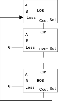
Idea #3.
Use the settings just mentioned so that the adder
computes A-B (and the mux throws it away).
Modify the HOB logic as follows (again it is easier to do this
modification for all bits, but just use the result from the
HOB).
- Bring out the result of the adder (before
the mux).
Call the output Set.
- Connect this Set output from the HOB, to
the Less input in idea #2 for the LOB.
- Thus the Less for the LOB is correctly set.
- Send a 0 to the Less input of the other bits.
- Since Less for the other bits should be
zero, Less is correct for all bits and we are done!
- The high level diagram of this maneuver is shown on the right.
Question: Why didn't I show a detailed diagram for
this method?
Answer: Because this method is not used.
Question: Why isn't the method used?
Answer: Because it is wrong!
Question: What is wrong?
Answer: It ignores overflows.
Consider the following 4-bit (instead of 32-bit) example.
- Try slt on -6 and +5.
- True subtraction gives -11.
- The negative sign in -11 indicates (correctly) that -6 <
+5.
- But 4-bit subtraction gives a positive result (and
asserts overflow).
- Hence the Set output of the hob is zero and we send
that to the Less input of the lob.
- Hence the circuit yields zero for slt given inputs -6 and
+5, thereby claiming that -6 is not less than 5.
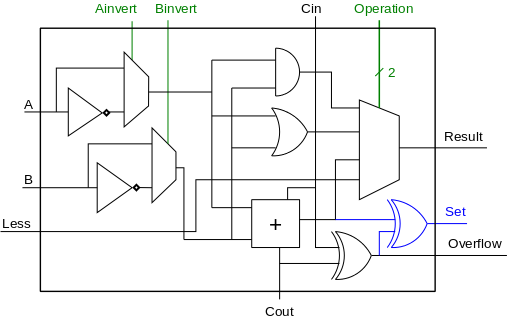
The Corrected 1-bit Cell for Set-Less-Than
To fix the above problem and get the final version of slt we need
to use the correct the rule for less than
rather than the
simple, but incorrect rule, the sign bit of A-B is 1
.
This simple rule ignores overflows and gives the wrong answer
whenever an overflow occurs.
Homework: Figure out
the correct rule, i.e. a non-pictorial version of problem B.24.
Hint: When an overflow occurs, the sign bit is definitely wrong.
An even bigger hint is that the diagram on the right shows the
correct calculation of Set in the HOB.
This is a case where explaining a bug is harder than fixing
it.
Once again we will use the enhanced 1-bit cell for all 32
bits even though only the LOB needs to calculate Set and
only the HOB needs to have a Less input.
Lab 3 Part 2: Enhance
your solution to part 1 to include the MIPS extensions:
NOR, Overflow, and SLT.
The External Interface of the 1-bit Cell
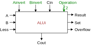
Recall that our goal is a 32-bit ALU.
It will contain 32 of the 1-bit ALUs we have just constructed.
When drawing the larger structure, we want to hide the details of
the individual 1-bit cells.
Thus when drawing the 32-bit ALU,we draw the 1-bit structure as
shown on the right, which shows only the external
interface and hides the internal details.
In the pictures below, to save space, I sometimes omit the labels
on the interfaces of the internal structures.
I try to ensure that they are in the same order as in the picture on
the right (let me know of any bugs you see) and try to have enough
information in the picture so that you do not need to know the
order.
Equality Detection
The last remaining feature we need is the ability to detect if
A = B, i.e., if A-B = 0.
Checking if all the bits are zero, is just a large NOR, which is
conceptually trivial, but does require some long wires.
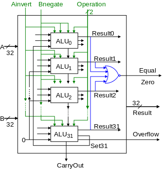
The Final Result
The final 32-bit ALU is shown on the right.
Note that all 32 1-bit cells are identical;
it is only the inter-cell wiring that differs.
This is important!
Lab 3 Part 3: Extend
your 1-bit solution as shown on the right (but again only 6 bits not
32).
The following additional points are worth noting.
CarryIn Missing
Although each 1-bit cell has 4 inputs
(Ainvert, Binvert, Cin, Operation),
the entire 32-bit ALU has only 3 inputs
(CarryIn is not present).
For all bits except the LOB, Cin is wired to Cout
of the preceding bit.
For the LOB, Cin is the same as Binvert.
So we define a single external line Bnegate, which is sent
to Binvert for every 1-bit alu and is also sent to
Cin of the LOB.
Thus there is no CarryIn signal needed.
All Bits the Same Internally
Again note that the internal
structure of all 32 1-bit cells are identical, i.e., all the bit
cells have the same circuit.
Therefore, only one bit cell needs to be specified in VLSI and,
perhaps more importantly, only one bit cell needs to be tested!
This means that every bit cell produces every output even though
some outputs are needed only for certain cells.
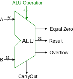
The lob and hob have special external wiring; the
other 30 bits have the same external wiring.
ALU Symbol
To the right we see the symbol that is used for an
ALU.
Although this shape symbol is always used, the exact operations
performed, the control lines used, and the outputs differ from one
implementation to another (for example set-less-than is mips
specific).
Note that we have combined the two 1-bit control lines
(Ainvert and Bnegate) together with the 2-bit
Operation control line into a single 4-bit control line
called ALUOperation.
The book uses the label Zero for the middle
output.
I believe a better label would be Equal since the output
is actually the Boolean value A==B (which is computed as
(A-B)==0)).
I use the term Equal Zero, rather than Equal,
to ease a comparison with the book.
Setting the Control Lines
| function | 4-bit cntl | Ainv | Bneg | Oper |
| AND | 0000 | 0 | 0 | 00 |
| OR | 0001 | 0 | 0 | 01 |
| ADD | 0010 | 0 | 0 | 10 |
| SUB | 0110 | 0 | 1 | 10 |
| SLT | 0111 | 0 | 1 | 11 |
| NOR | 1100 | 1 | 1 | 00 |
The ALU can directly perform the following MIPS instructions by
setting the control lines as indicated in the table on the right.
- AND
- OR
- ADD
- SUB
- SLT (set on less than)
- NOR
Remark: We have developed the logic needed to
implement 6 machine instructions.
The technical term is that we have developed the data path.
That is one of three tasks needed for a full implementation.
The other two are:
- Given the actual machine instruction, we need to determine the
value for ALUOperation.
This is not too hard and involves no new concepts, as we shall
see.
- We need to implement the register file since the operands for
all these instructions are registers.
Although this is also not terribly difficult it definitely
requires an important new concept:
sequential logic, i.e, circuits with memory or
state.
Before we do either of these tasks, we will learn a much faster
method for addition (and subtraction).
Defining the MIPS ALU in Verilog
B.6: Faster Addition: Carry Lookahead
The alu above is not used in practice since it is too slow.
The fundamental problem is that calculating bit i
of the sum requires the carry out from bit i-1.
For this reason the above alu is said to perform a
ripple carry
since the carry computation ripples along from
the lob to the hob.
Thus, for a 64-bit addition, the hob will take a long time to
compute.
The adder we will study next is much faster than the ripple adder
we did before, especially for wide (i.e., many bit) addition.
(With two's complement addition, any adder can subtract by
complementing the bits of the subtrahend, asserting CarryIn, and
adding—as we did above.
Fast Carry Using Infinite
Hardware
This is a simple (theoretical) result, but not practical.
- An adder is a combinatorial circuit hence it can be constructed
with two (or three if you count the bubbles) levels of logic.
Done.
- Consider 32-bit (or 64-bit, or 128-bit, or N-bit) addition, R=A+B.
- This is a logic function with 32+32=64 binary inputs.
- It has 33 outputs (Sum and the final
CarryOut).
- Hence it can be expressed by a truth table having
264 rows and 64+33=97 columns.
- This is a gigantic truth table with
264×97=1789334175149826506752 entries,
but nonetheless finite.
- Naturally 64-bit addition is much
worse.
- The above is a worst case analysis.
The actual circuit for addition is probably not quite as
bad, but still completely impractical for real 64-bit
adders
- Here is another way.
- Each of the 1-bit adders we built was fast (just a few
gate delays); the trouble was that the Cins to the
upper order bits took a long time to calculate.
We can calculate all the Cins from just the inputs
a, b, and CarryIn=Cin0
using two levels of logic (and some algebra).
- For simplicity I will write
c0 for CarryIn=Cin0,
c1 for Cin1,
c2 for Cin2, etc.
- Also for simplicity I write the inputs as
a and b (rather than as
A and B).
- c0 is an input.
- c1 = a0 b0 + a0 c0 + b0 c0
-
c2 = a1 b1 + a1 c1 + b1 c1
= a1 b1 + a1 a0 b0 + a1 a0 c0 + a1 b0 c0 + b1 a0 b0
+ b1 a0 c0 + b1 b0 c0
- c3 = a2 b2 + a2 c2 + b2 c2 = ...
(substitute for c2)
- etc.
- Again this gives 2-levels of logic to generate each carry
from just the inputs.
And again the result is impractical since there will be many
ANDs each with many inputs and (for each carry) a giant
OR.
- With these formulas for the carries, we can get
disjunctive normal forms for the sums.
For example
s2 = a2 b2 c2 + a2 b2' c2' + a2' b2 c2' + a2' b2' c2
= a2 b2 (formula for c2) + a2 b2'
(formula for c2)'
+ a2' b2 (formula for c2)' + a2' b2'
(formula for c2) = ....
- So theoretically fast, but impractical, circuits are easy to
derive.
Fast Carry Using the First Level of Abstraction: Propagate and Generate
At each bit position we have two input bits ai
and bi as well as a CarryIn input.
We now define two other bits called propagate
(pi=ai+bi) and generate
(gi=aibi), which have the
following properties.
- We can calculate the carries fairly quickly given p
and g (to be shown below).
- We can calculate p and g very quickly (one
gate delay).
- It is crucial to note that p
and g depend only on a and b.
- Specifically p and g do NOT
depend on c.
- Hence p and g for all bits
can be calculated at once, there is
no
ripple
effect.
The reason for the name propagate
is that if p is
true, the current bit will propagate a carry from its input to its
output.
More precisely:
  if (pi) then
     if (there is a carry in to bit i) then
        there is a carry out from bit i
  else
     there is no carry out from bit i
The reason for the name generate
is that if g is
true, then the current bit will generate a carry out (independent of
the carry in).
More precisely:
  if (gi) then {
     there is definitely a carry out from bit i
  }
Another way to say it is that at each bit i
  cout = ab + acin + bcin
       = ab + (a+b)cin
       = g  + pcin
So cout=1 if
either
g=1
or
both p=1 and cin=1
These key formulas are quite simple, but
are very useful.
To repeat:
Generate:
gi = ai·bi
Propagate:
pi = ai+bi
The diagram on the right, from P&H, gives a
plumbing analogue for generate and propagate.
The top pipe corresponds to a 1-bit adder, the middle pipe to a
2-bit adder, and the bottom pipe to a 4-bit adder.
A larger version of the diagram is
here.
(The plumbing diagrams in these notes are from the 2e; the colors
changed between additions, but the contents are the same.)
The point is that liquid enters the main pipe if
either the initial CarryIn or one of the generates is true.
The water exits the pipe at the lower left (i.e.,
there is a CarryOut for this bit position) if all the propagate
valves are open from the lowest liquid entrance to the exit.
Given the generates and propagates, we can calculate all the
carries for a 4-bit addition as follows (recall that
c0=Cin is an input).
These formulas correspond directly to the plumbing picture on the
right.
For simplicity, I will stop writing subscripts smaller and
subtended.
  c1 = g0 + p0 c0
  c2 = g1 + p1 c1 = g1 + p1 g0 + p1 p0 c0
  c3 = g2 + p2 c2 = g2 + p2 g1 + p2 p1 g0 + p2 p1 p0 c0
  c4 = g3 + p3 c3 = g3 + p3 g2 + p3 p2 g1 + p3 p2 p1 g0 + p3 p2 p1 p0 c0
Thus we can calculate c1 ... c4 in just two additional
gate delays given the p's and g's.
(We assume one gate can accept up to 5 inputs).
Since we get gi and pi after one gate delay, the
total delay for calculating all the carries is 3 gate delays.
This includes calculating c4=CarryOut.
Start Lecture #6
Note: The above formulas are for 4-bit arithmetic.
An important point is that, if the numbers have more bits, the
formulas will still use only two levels of
logic but the number of inputs to each AND and OR
will get bigger (a very important but
).
We now show that first calculating p and g, speeds up addition.
- We can calculate the p's and g's in one gate delay.
- After calculating the p's and g's we can calculate the carries
in 2 additional gate delays using the above formulas.
- Thus 3 gate delays after we start we have all four carries.
- After calculating the carries we can calculate the sum in 2 gate
delays since now each bit is independent.
- Thus 5 gate delays after we start, we are finished.
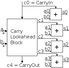
We illustrate the separate calculations of the carries and the sum
in the diagram on the right.
- The
Carry Lookahead Block
has inputs a,
and b and the carry in.
The block calculates the pis
and gis internally (not shown in the
diagram) and then calculates the carries, which are the outputs of
the block.
We have seen above that the block requires 3 gate delays.
- Each small box labeled
+
is the part of a full
adder that calculates the sum
      si = ai⊕bi⊕ci
         = ai·bi·ci + ai·bi'·ci' +
           ai'·bi·c' + ai'·bi'·c
Note that the carries are not calculated by
these boxes; instead they are inputs to those boxes.
- The small boxes require 2 gate delays.
- Note the division of labor: The carry lookahead block calculates
the pis and gis, and
from these calculates the carries (the cis);
the other blocks calculate the sums
(the sis) given the
carries.
In summary, for 4-bit addition, 5 gate delays after we are
given a, b and the Carry-In, we have
calculated s and the Carry-Out using a modest amount of
realistic (no more than 5-input) logic.
How does the speed of this carry-lookahead adder CLA compare to our
original ripple-carry adder?
- We have just seen that a 4-bit CLA completes its calculation
in 5 gate delays.
- The ripple-carry adder is composed of four 1-bit full adders
(FAs).
- Each FA needs only two gate delays.
Our design was slower, but we were aiming for clarity not speed.
It is a combinatorial circuit so of course theoretically it can
be done in 2 gate delays (assuming the bubbles are free) and the
design you get in this way is practical as well.
- But the calculation of bit i takes
two gate delays starting from when the
calculation of the previous CarryOut is finished since
bit i needs the CarryOut of bit i-1 as its
own Carry-In.
- Thus the time required for a 4-bit adder is 4*2=8 gate
delays.
- Summary: With 4-bit addition CLA wins 5 to 8.
Lab 3 Assigned:
Due in one week.
Fast Carry Using the Second Level of Abstraction
We have finished the design of a 4-bit CLA.
Our next goal is a 16-bit fast adder.
Let's consider, at varying levels of detail, five possibilities.
- Ripple carry.
Simple, easy to do, but not fast (16*2=32 gate delays).
- General 2 levels of logic.
Always applicable and very fast (2 gate delays).
We know how to do it, but it is not practical.
- Extend the above 4-bit CLA design to 16 bits.
- Possible.
- We could do it, but some gates would have many inputs; this
is the very important but we referred to
above.
- In particular, the formula for c4 above
has one AND with 5-inputs and the OR also has 5 inputs.
So c5 would have a 6-input AND and a
6-input OR.
Finally, c16 would have a 17-input AND,
and a 16-input AND, etc and a 17-input OR.
- Hence we would need a tree to reduce the input count and
this tree would slow down the computation.
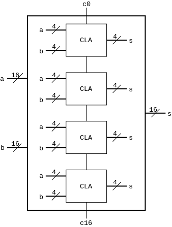
- Put together four of the 4-bit CLAs.
Shown in the diagram to the right is a schematic of our 4-bit
CLA and a 16-bit adder constructed from four of them.
- As black boxes, both ripple-carry adders and
carry-lookahead adders look the same, i.e., they have the same
inputs and outputs.
- As shown we can simply put four CLAs together and let the
Carry-Out from one be the Carry-In of the next.
That is, we could put these CLAs together in a ripple-carry
manner to get a hybrid (carry-lookahead/ripple-carry) 16-bit
adder.
- Since the Carry-Out is calculated in 3 gate delays, the
Carry-In to the high order 4-bit adder is calculated in
3*3=9 gate delays.
- Hence the overall Carry-Out takes time 9+3=12 and the high
order four bits of the sum take 9+5=14.
The other bits take less time.
- So this mixed 16-bit adder takes 14 gate delays compared
with 2*16=32 for a straight ripple-carry 16-bit adder.
- Note that this hybrid structure is not a
true 16-bit CLA because the 4-bit structures are ripple-carry
connected.
- Be more clever and put together the 4-bit CLAs in a
carry-lookahead manner.
One could call the result a 2-level CLA.
- We have 33 inputs
a0,...,a15;
b0,...b15;
c0=Carry-In
- We want 17 outputs
s0,...,s5; c6=Carry-Out
- As before, we are assuming a gate can accept up to 5 inputs.
It is important that the number of inputs per gate does not
grow with the number of bits in the addends.
- If the technology available supplies only 4-input gates
(instead of the 5-input gates we are assuming), we would use
groups of three bits rather than four.
- This will take us some time to develop and is our next
goal.
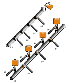
Super Propagate
and Super Generate
We start the adventure by defining super propagate
and
super generate
bits.
From these super propagates and super generates, we can calculate the
super carries, i.e. the carries for the four 4-bit adders.
We will use four of the 4-bit CLAs to form our 16-bit CLA but we
want to calculate all the Carry-In's to the 4-bit CLAs at once
NOT in a ripple-carry manner as we did in the
hybrid (carry-lookahead/ripple-carry) adder.
This is terrific!
These super carries are what we need to combine four 4-bit CLAs into
a 16-bit CLA in a carry-lookhead manner.
Recall that the hybrid approach suffered because the carries from
one 4-bit CLA to the next (i.e., the super carries) were calculated
in a ripple carry manner.
Since it may not be completely clear how to combine the pieces so
far presented to get a 16-bit, 2-level CLA, I will give a pictorial
account very soon.
In fact, the pictures will show how to get a 4n-bit CLA
for any n≥0 (1-bit, 4-bit, 16-bit, 64-bit, ...).
How Fast is the New Design?
Before the pictures, let's assume the pieces can be put together
and see how fast the 16-bit, 2-level CLA actually is.
Recall that we have already seen two practical 16-bit adders: A
ripple carry version taking 32 gate delays and a hybrid structure
taking 14 gate delays.
If the 2-level design isn't faster than 14 gate delays, we won't
bother with the pictures.
Remember we are assuming 5-input gates.
We use lower case p, g, and c for propagates, generates, and
carries; and use capital P, G, and C for the super- versions.
The procedure is:
- Calculate the p's and g's (lower case) in 1 gate delay (as with
the 4-bit CLA).
- Calculate the P's one gate delay after we have the p's, i.e., 2
gate delays after we start.
- The G's are determined 2 gate delays after we have the g's and
p's, i.e., 3 gate delays after we start.
- The C's are determined 2 gate delays after the P's and G's,
i.e., 5 gate delays after we start.
- Now the C's are sent back to the 4-bit CLAs, which have already
calculated the p's and g's.
The c's are calculated in 2 more
gate delays (7 total) and the s's 2 more after that (9 total).
Since 9<14, let the pictures begin!
Putting the Pieces Together: a Pictorial Account
Step 1: Minor Surgery on the 4-bit CLA
We produce a 4-bit CLA-PG, which is a small
enhancement to the 4-bit CLA already shown.
The name is not standard.
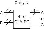
Combining Four 4-bit CLA-PG's with a CL Block
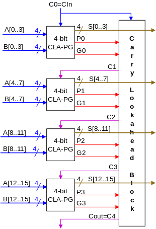
Next we put four of these 4-bit CLA-PGs together
with a new structure called a Carry Lookahead Block (CL Block) that
calculates the carries needed by the 4-bit CLA-PGs using the P's,
G's and Cin=C0.
The result will be a 16-bit CLA!
We will see the diagram on the right twice, this
first time don't worry how many gate delays are required for each
calculation.
We will study that the second time through the diagram.
The colors of the lines indicate the order in which the calculations
are performed.
- We are given in blue A0...A15 and
B0..B15.
We are also given Cin, the carry in to the 16-bit
addition.
- These 32 As and Bs are divided in to four groups of four pairs
each with each group sent to a 4-bit CLA-PG.
- Each CLA-PG calculates, 4 pi and 4 gi the
one bit propagate and generate bits.
These 8 values are used in the next step but are not sent out of
the box.
- Using its p's and g's, each box calculates P and G, the super
propagate and generate bits of the 4-bit unit and sends these two
bits (using red lines) to the CL-block.
- The CL-block has now received nine inputs, 4Ps, 4Gs, and
Cin the overall carry in.
It calculates the four super carries C1...C4
and sends them back in magenta to the corresponding 4-bit
CLA-PGs.
The formulas for the Cs are above but I repeat them here.
  C0 = Cin
  C1 = G0 + P0 Cin
  C2 = G1 + P1 C1 = G1 + P1 G0 + P1 P0 Cin
  C3 = G2 + P2 C2 = G2 + P2 G1 + P2 P1 G0 + P2 P1 P0 Cin
  C4 = G3 + P3 C3 = G3 + P3 G2 + P3 P2 G1 + P3 P2 P1 G0 + P3 P2 P1 P0 Cin
- The CLA-PGs have (long ago) calculated their p's and g's.
Once they receive their magenta carry in's they calculate their
(lower case) carries and 4-bit sums and send the latter out in
brown.
- These brown sums form the desired 16-bit sum and together with
the overall carry out Cout complete the operation.
How Fast is it?
As mentioned the first time we saw the diagram on
the right, the color of the wires indicate when the values are
calculated.
As we have seen:
- The blue lines are inputs.
- Then the red lines are calculated.
- Then the magenta.
- Finally the brown.
The last four statements are sloppy.
Gates are always calculating their outputs from
their inputs.
When we say a value is calculated in k gate delays, we mean that
the value is correct k gate delays after the inputs are correct.
A more accurate version of the fout points above would be
- The blue lines are input, which are assumed to be
valid when we start the addition.
- The little p's and g's (which are not shown) are valid 1 gate
delay after the blue lines are valid.
The red lines are valid 2 gate delays after the the little p's and
g's are valid (actually the capital Ps needs only 1 gate delay,
but we use the Ps and Gs together so need to wait for the
Gs).
Summary: the red lines are valid 3 gate delays after we
start.
- The magenta lines are valid 2 gate delays after the
red; so they are valid 5 gate delays after the start.
- The brown lines are valid 4 gate delays after the
magenta (2 gate delays to calculate the c's—note
lower case, then two more for the Ss); so they are valid
9 gate delays after the start.
Note: It is crucial that all the Ci's
are calculated at once.
For example, it is not true that C3
depends on C2.
Enhancing the CL Block
We are not done with the CL Block since our ultimate
goal is to construct CLAs for any power-of-4 number of bits using
this one CL Block.
Specifically, again assuming 5-input gates, we want the
exact same CL Block to be used for a 4-bit
(1-level) CLA; a 16-bit (2-level) CLA; a 64-bit (3-level) CLA; a
256-bit (4-level) CLA, etc.
In fact, we will go back further and construct a 1-bit (0-level)
CLA, from which the 4-bit (1-level) CLA is built, again using the
identical CL-Block.
Note that I do not call the CL Block a 4-bit CL Block or a 16-bit
CL block.
This one block works for all (power of 4) sizes.
More on this latter
Moreover, when going from an 4n-bit (n-level)
CLA to a 4n+1-bit (n+1-level) CLA, there will be
no new logic used.
Specifically, we want a 64-bit (3-level) CLA to be composed of four
16-bit (2-level) CLAs, one additional CL Block
(identical to those in the smaller constituent
CLAs), some wires, and nothing else.
In the previous diagram we used a CL Block to assemble a
16-bit CLA from four 4-bit CLAs, but did not prepare for
constructing a 64-bit CLA from four of these 16-bit CLAs.
For that reason the CL block did produce Pout
and Gout (note that each 4-bit CLAs used did
output a P and a G, which were used when constructing a
16-bit CLA).
In general, when constructing a CLA using the CL Block, there are
actually three sizes of CLAs that are relevant (so far we have only
dealt with two of the three).
- The previous size CLA, i.e., the size of the
constituent CLAs (4-bit in the diagram above).
- The current size, i.e., the size being
constructed (16-bit above).
- The next size, i.e., the size for which the CLA under
construction will be a constituent.
The diagram above did not support constructing
the next size CLA (64-bit), a defect soon to be remedied.
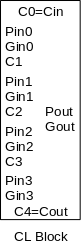
The full CL Block is drawn on the right and contains two
outputs not shown or used previously, Pout
and Gout.
This Block has the following 9 inputs.
- 4 propagate bits from the previous size
Pin0, Pin1,
Pin2, and Pin3.
- 4 generate bits from the previous
size, Gin0, Gin1,
Gin2, and Gin3.
- The Carry-In C0=Cin.
It has the following 6 outputs
- Four carries C1, C2,
C3, and C4.
The first three of which are used by the constituent
CLAs of the previous size.
- C4=Cout is an output of the current size CLA.
- Pout and Gout, the propagate and
generate to be used in the next size CLA.
These outputs are calculated from the following,
previously studied, formulas.
         C1 = Gin0 + PinO Cin
         C2 = Gin1 + Pin1 Gin0 + Pin1 Pin0 Cin
         C3 = Gin2 + Pin2 Gin1 + Pin2 Pin1 Gin0 + Pin2 Pin1 Pin0 Cin
  Cout = C4 = Gin3 + Pin3 Gin2 + Pin3 Pin2 Gin1 + Pin3 Pin2 Pin1 Gin0 + Pin3 Pin2 Pin1 Pin0 Cin
  Pout = Pin3 Pin2 Pin1 Pin0
  Gout = Gin3 + Pin3 Gin2 + Pin3 Pin2 Gin1 + Pin3 Pin2 Pin1 Gin0
Building CLAs Using the CL Block
It is now time to validate the claim that all (power of 4) sizes of
PLAs can be built (recursively) using the CL Block.
1-bit CLA-PG
A 1-bit CLA is just a 1-bit adder.
With only one bit there is no need for any lookahead
since
there is no ripple
to try to avoid.
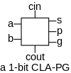
However, to enable us to build a 4-bit CLA from the 1-bit version,
we actually need what we call CLA-PG1, a 1-bit CLA-PG.
As shown on the right, the 1-bit CLA-PG has three inputs
a, b, and cin.
It produces 4 outputs s, cout, p, and g.
We have given the logic formulas for all four outputs previously,
but here they are again.
     s = a b cin + a b' cin' + a' b cin' + a' b' cin    odd number bits are 1
  cout = a b + a cin + b cin                            at least two bits are 1
     p = a + b
     g = a b
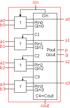
4-bit CLA-PG
A 4-bit CLA-PG is shown as the red portion in the
figure to the right.
It has nine inputs: 4 a's, 4 b's,
and cin and must produce seven outputs: 4 s's,
cout, p, and g (recall that the
last two were previously called the super propagate and super
generate respectively).
The tall black box is our CL Block.
The question is, what must the ith ?
box do in
order for the entire (red) structure to be a 4-bit CLA-PG?
.
- The ? box must produce si, the ith
bit of the desired sum.
But this is easy since the box
receives ai, bi, and
ci (c0 is cin).
The formula (repeated from above) is that an odd number of inputs
must be set, namely
si = ai bi ci +
ai bi' ci' +
ai' bi ci' +
ai' bi' ci
- The ? box must produce pi and gi for the
CL Block to consume.
But that is also easy since it has as
input ai and bi, and
      pi = ai + bi
      gi = ai bi
So the ? box is just a 1-bit CLA-PG, which we sometimes write as
CLA1 or CLA-1 for short.
Question: Why is this last statement wrong?
Answer: The ? box is only a (large) subset of a
1-bit CLA-PG.
Question: What is missing?
Answer: The ? box doesn't need to produce a carry
out since the Cl-block produces all the carries.
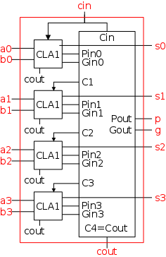
So, if we want to say that the 4-bit (1-level) CLA-PG is composed
of four 1-bit (0-level) CLA-PGs together with a CL Block, we must
draw the bottom picture shown on the right.
The difference is that the bottom picture makes explicit that the ?
box produces cout, which is then not used.
This situation will occur for all sizes.
For example, either picture on the right for a a 4-bit
CLA-PG produces a carry out since all 4-bit full adders do so.
However, a 16-bit CLA-PG, built from four of the 4-bit units and a
CL Block, does not use the carry outs produced by the four 4-bit
units.
We have several alternatives.
- Don't mention the problem of the unused cout.
This is probably the most common solution, but too late for us
since I already mentioned it.
- Draw the top version of the diagram (without the unused
cout's) and delcare that a CLA-PG doesn't produce a
carry out.
It seems weird (to me, at least) that a CLA-PG doesn't have all
the outputs of a full adder.
- Draw the top version of the diagram and admit that a level k
CLA-PG doesn't really use four level k-1 CLA-PG's, but instead
uses 4 copies of a large subset of a level k CLA-PG.
I don't like this since it means you need to reverify the large
subset.
- Draw the bottom version of the diagram.
This seems reasonable to me.
- Draw the top version of the diagram, but view it as an
abbreviation of the bottom version.
As another abbreviation, we will henceforth say CLA when we mean
CLA-PG.
Summary:
A 4-bit CLA (meaning CLA-PG) is composed of
- Four 1-bit CLAs
- One CL block
- Wires
- Nothing else
Start Lecture #7
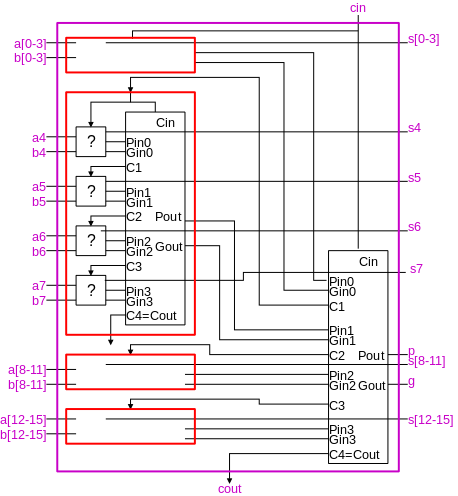
16-bit CLA-PG
Now take four of these 4-bit adders and use the
identical CL Block to get a 16-bit
adder.
The picture on the right shows one 4-bit adder (the tall red box)
in detail.
The other three 4-bit adders are just given schematically as small
empty red boxes.
The CL Block is also shown and is wired to all four 4-bit
adders.
The complete (large) picture is
shown here.
Summary:
A 16-bit CLA is composed of
- Four 4-bit CLAs
- One CL block
- Wires
- Nothing else
64-bit CLA-PG
To construct a 64-bit CLA no new components are needed.
That is, the only components needed have already been constructed.
Specifically you need.
- Four magenta boxes, identical to
the one just constructed.
- One additional CL Block, identical
to the one just used to make the magenta box (which is also
identical to the one used to make
the red box).
- Wires to connect these five boxes.
Summary:
A 64-bit CLA is composed of
- Four 16-bit CLAs
- One CL block
- Wires
- Nothing else
When drawn (with a brown box) a 64-bit CLA has 129 inputs
(64+64+1) and 67 outputs (64+1+2).
256-bit CLA-PG
Once again no new components are needed, just
- Four brown boxes, identical to
the one just constructed.
- One additional CL Block, identical
to the one just used to make the brown box.
- Wires to connect these five boxes.
Summary:
A 256-bit CLA is composed of
- Four 64-bit CLAs
- One CL block
- Wires
- Nothing else
etc
For any n≥0 a 4nn-bit CLA-PG can
be constructed from
- n 1-bit CLA-PGs.
-
40 + 41 + 42 +
... 4n-1 = (4n-1) / 3
CL Blocks.
- Wires.
- Nothing else.
Homework: How many gate
delays are required for our 64-bit CLA-PG?
How many gate delays are required for a 64-bit ripple carry adder
(constructed from 1-bit full adders)?
Note: CLAs greatly speed up addition, reducing the
number of gate delays for n-bit addition
from Θ(n) to Θ(log(n)).
Shifters
MIPS (and most other) processors have shift (and rotate)
instructions.
We could easily extend the ALU to do 1-bit shift/rotates (i.e.,
shift/rotate a 32-bit quantity by 1 bit), and then perform an n-bit
shift/rotate as n 1-bit shift/rotates.
This is not done in practice.
Instead a separate structure, called a barrel shifter is
built outside the ALU.
Note: Barrel shifters, like CLAs, are of
logarithmic complexity.
Start Lecture #8
*** Big Change Coming ***
B.A Sequential Circuits, Memory, and State
Why do we need state?
- Memory (i.e., ram not just rom or prom).
- Counters.
- Reducing gate count.
- For example, using only combinatorial/combinational circuits
(as we have up till now), multiplying two n-bit numbers
requires about n2 gates (think about how
you multiply n-digit numbers.)
- However, with sequential logic (and hence state),
multiplication can be done with about n gates, as we shall see
later in the course.
B.7: Clocks
Assume you have a physical OR gate.
Assume the two inputs are both zero for an hour.
At time t one input becomes 1; the other one never changes.
The output will oscillate for a while before
settling on 1.
We want to be sure we don't look at the answer before its ready.
This will require us to establish a clocking methodology,
i.e., an approach to determining when data is valid.
First, however, we need to review again some ...
Terminology
Micro-, Mega-, and Friends
Nano means one billionth, i.e., 10-9.
Micro means one millionth, i.e., 10-6.
Milli means one thousandth, i.e., 10-3.
Kilo means one thousand, i.e., 103.
Mega means one million, i.e., 106.
Giga means one billion, i.e., 109.
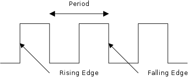
Frequency and period
Consider the idealized waveform shown on the right.
The horizontal axis is time and the vertical axis is (say) voltage.
If the waveform repeats itself indefinitely (as the one on the
right does), it is called periodic.
The time required for one complete cycle, i.e., the
time between two equivalent points in consecutive cycles, is called
the period.
Since it is a time, period is measured in units
such as seconds, days, nanoseconds, etc.
The rate at which cycles occur is called the
frequency.
Since it is a rate, frequency is measured in units
such as cycles per hour, cycles per second, kilocycles per
micro-week, etc.
The modern (and less informative) name for cycles per second is
Hertz, which is abbreviated Hz.
Prediction: At least one student will confuse frequency and periods
on the midterm or final and hence mess up a gift question.
Please, prove me wrong!.
Make absolutely sure you understand why
- A kilohertz clock is (a million times) faster
than a millihertz clock.
- A clock with a kilosecond period is (a million
times) slower than one with a millisecond period.
Edges
Look at the diagram above and note the rising
edge and the falling edge.
We will use edge-triggered logic, which means that state
changes (i.e., writes to memory) occur at a clock
edge.
Each of our designs will either
- Have all state changes occur at rising edges or
- Have all state changes occur at falling edges.
The edge on which changes occur (either the rising or falling edge)
is called the active edge.
For us, choosing which edge is the active edge is basically a coin
flip.
In real designs the choice is governed by the technology used.
Some designs permit both edges to be active.
Examples include DDR (double data rate) memory and double-pumped
register files.
This permits a portion of the design to run at effectively twice the
speed since state changes occur twice as often
Synchronous system
Now we are going to add state elements (memory) to the
combinational circuits we have been using previously.
Remember that a combinational/combinatorial circuit has its outpus
determined solely by its input, i.e. combinatorial circuits do not
contain state.
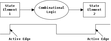
State elements include state (naturally).
- That is, state elements are memory.
- A state elements has the clock as an input.
- Since we are using edge-triggered memory, these elements change
state only at the active edge of the clock.
- They always produce output, which is based on the current
state.
- It is our job to ensure that all signals written to state
elements are valid at the time of the active edge.
- For example, if the cycle time (of the clock) is 10ns, the
designer must ensure that combinational circuit used to compute
new state values completes (i.e., has settled on the correct
output) within 10ns.
- So state elements change at the active edge, the combinatorial
circuit stabilizes between active edges.
- It is actually a little more complicated
(setup and hold times must be accounted for).
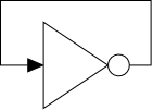
Combinatorial circuits can NOT contain loops.
For example, imagine an inverter with its output connected to its
input.
So if the input is false, the output becomes true.
But this output is wired to the input, which is now true.
Thus the output becomes false, which is the new input.
So the output becomes true ... .
Sequential circuits, however, can and often
do contains loops.
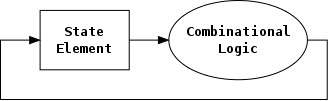
- Think of state elements as registers or memory.
- Can have loops like at the right.
- For example imagine the assembler instruction
add-register r1=r1+r1
The state element is register number 1 and the combinatorial
circuit is a full adder.
B.8: Memory Elements: Flip-Flops, Latches, and Registers
We will use only edge-triggered, clocked memory in our
designs as they are the simplest memory to understand.
So our current goal is to construct a 1-bit, edge-triggered, clocked
memory cell.
However, to get there we will proceed in three stages.
- We first show how to build unclocked memory.
- Then, using unclocked memory, we build
level-sensitive clocked memory and stop using unclocked
memory.
- Finally from level-sensitive clocked memory we
build edge-triggered clocked memory and stop using
level-sensitive clocked memory.
Unclocked Memory
The only unclocked memory we will use is a so called S-R latch
(S-R stands for Set-Reset).
Note: When we define the term latch
below,
we will see that the S-R latch is not technically a latch.
The circuit for an S-R latch is on the right.
As we can see the S-R latch is constructed from a pair
of cross-coupled
nor gates.
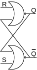
Since the S-R latch has two single-bit inputs, there are four
possible input combinations.
- We never assert both S and R at the same time.
- When S is asserted (i.e., S=1 and R=0):
- The latch is Set (that's why it is called S).
- Q becomes true (Q is the output of the latch).
- Q' becomes false (Q' is the complemented output).
- When R is asserted:
- The latch is Reset.
- Q becomes false.
- Q' becomes true.
- When neither one is asserted:
- The latch retains its value, i.e. Q and Q' stay as they
were.
- This last statement is the memory aspect.
We will use an S-R latch only once.
Specifically we use it right now to construct a D-latch.
Clocked Memory: Flip-flops and Latches
For both flip-flops and
latches the output equals the value stored in the
structure.
Both have an input and an output (and the complemented output) and a
clock input as well.
The clock determines when the internal value is set to the current
input.
For a latch, the output can change whenever the clock is asserted
(level sensitive).
For a flip-flop, changes occur only at the active edge.
Unfortunately the terminology used is not perfect, the
S-R latch defined above
is unclocked memory and hence not a latch.
D latch
The D stands for data.
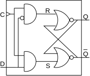
Note the following properties of the D latch circuit shown on the
right.
- The left part of the circuit uses the clock;
the right part is essentially an S-R latch.
- When the clock is high, S=D and R=D' so, Q, the output of the
latch, is D.
- When the clock is low, both R and S are forced low so the
outputs (Q and Q') don't change.
This means that whatever value Q last had when the clock was high,
is the value that Q will continue to have while the clock is
low.
That is, the last value before the clock went low
is stored in (and supplied by) the latch for the
duration of the time the clock remains low.
- The output changes when input changes and the clock is
asserted, that is the latch is level sensitive, it's
behavior depends on the level (asserted or deasserted) of the
clock.
Remember that we seek edge triggered logic.
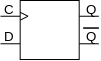
The abbreviated diagram on the right is how a D-latch is normally
drawn.
A D latch is sometimes called a transparent latch since,
whenever the clock is high, the output equals the input (i.e., the
input passes right through the latch).
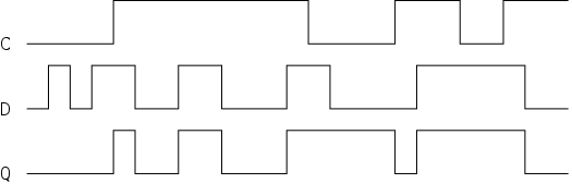
Traces
Note the following points illustrated by the traces
to the right.
We assume the stored value was initially low.
- The output follows the input when the clock is high.
- The output remains constant when the clock is low.
We won't use D latches in our designs, except right now to
construct our workhorse, the master-slave flip-flop, an
edge-triggered memory cell.
D or Master-Slave Flip-flop
This structure has been our goal.
It is an edge-triggered, clocked memory.
It is often referred to as a D-flop.
Again the D stands for data.
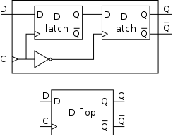
The circuit for a D flop is on the right and has the following
properties.
- The D flop is built from D latches, which are transparent.
- The flop, however, is not transparent.
Instead changes to the output occur only at the active edge, which
for the circuit in the diagram is the falling edge.
We shall see this shortly.
A D flop is sometimes called a master-slave flip-flop, with the
left latch called the master and the right the slave.
Note that the substructures reuse the same letters as the main
structure but have different meaning (similar to block structured
languages in the algol style).
The left D latch is set during the time the clock is asserted.
Remember that the latch is transparent, i.e. its output follows its
input when the clock is asserted.
But the right latch is ignoring its input at this time.
When the clock falls, the 2nd latch pays attention and the first
latch keeps producing whatever D was at fall-time.
Homework:
Move the inverter to the other latch.
What has changed?
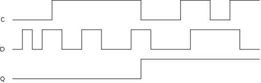
Traces
The picture on the right is for a master-slave
flip-flop.
As before we are assuming the output is initially low.
Note how much less wiggly the output is in this picture
than before with the transparent latch.
The only changes in the output occur when the clock falls; that is
the output can only change once per cycle.
Homework: Which code
better describes a flip-flop and which a latch?
For the one describing a flop is the active edge the rising or
falling edge?
  repeat {
     while (clock is low) {do nothing}
     Q=D
     while (clock is high) {do nothing}
  } until forever
or
  repeat {
     while (clock is high) {Q=D}
  } until forever
Setup and Hold Times
Actually for a D flop to work correctly, the input D must remain
constant for some time around the active edge.
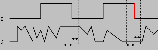
- The set-up time before the edge.
- The hold time after the edge.
- The picture on the right shows the setup and hold times.
- It is crucial when building circuits with flip flops that D is
stable during the interval around the active edge including the
setup and hold times.
- Note that D is wild outside this critical interval, but that
is OK.
- We will not be emphasizing setup and hold requirements in this
course.
Registers
A register is basically just an array of D flip-flops.
For example a 32-bit register is an array of 32 D flops.
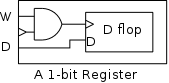
What if we don't want to write the register during a particular
cycle (i.e. at the active edge of a particular cycle)?
As shown in the diagram on the right, we introduce another input,
the write line, which is used to gate the clock
.
If the write line is high forever, the clock input to the register
is passed right along to the D flop and hence the input to the
register is stored in the D flop when the active edge occurs, which
for us is the falling edge.
That is, the register is written every cycle.
If the write line is low forever, the clock to the D flop is always
low so has no edges.
Thus the register is never written.
Now that we understand what happens if the write line is constant,
either always high or always low, we must ask what happens if we
change the write line from high to low or vice versa.
We do not change the write line when the (external) clock is high
since that would cause extra edges to be passed to the D-flop.
Since we do not want to introduce extra edges, our
first idea is to arrange to change the write line only when the
clock is low.
This, however, is not such a good idea!
Recall that the active edge is the falling edge.
Thus, when the clock is low, we are in the first half of the cycle
and we must have determined, during this first half cycle, whether
we want to write at the end of the cycle.
Hence, we have only 1/2 a cycle to decide.
It would be better to arrange everything so that we can change the
write line when the clock is high instead of when the clock is low.
That way we must know the value and write it during the second half
of the cycle.
Thus we can use nearly the entire cycle to decide whether to write
the register at the end of the cycle.
How can we do this?
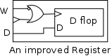
One way is to change the way we gate the clock.
Instead of ANDing the clock with the write line, we OR the clock
with the complement of the write line.
Now changing the write line when the clock is high does not
introduce an edge.
In this way the write line can be changed when the clock is high
without affecting the clock to the D-flop, i.e. we can decide
whether to write the register during the second half of the cycle.
The downside is that we must not change the write line during the
first half of the cycle when the clock is low.
However, it is much easier to meet a requirement to go slowly than
one to go fast.
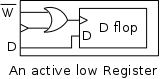
The same affect can be achieved in another manner as well.
Instead of having the register negate the write line W, we
essentially require that the users of the register do it.
Specifically, instead of having a write-register
input W, the
register has a don't-write-register
input W'.
The semantics is that the register is written (at the active,
falling, edge) if the don't write line,
is not asserted.
Such a register, which is depicted on the right, is often called
an active low
register since it is active when its W' input
is low (de-asserted).
Start Lecture #9
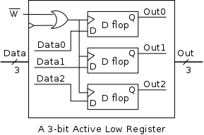
Multibit Registers
To implement a multibit register, just use multiple D flops.
As we did for adders, the Data input is shown as 3-bits wide
external to the multibit register but as three separate 1-bit lines
internally where the individual bits go separate D-flops.
This dual representation is also used for the 3-bit Out line.
Splitters again!
Register Files
A register file is just a set of registers, each one numbered.
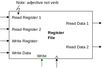
As shown in the figure on the right, when accessing a register
file, you supply the register number, the write line (asserted if
a write is to be done), and, if the write line is asserted, the
data to be written.
You can read and write same register during one cycle.
You read the old value and then the written value replaces this
old value for subsequent cycles.
Often have several read and write ports so that several registers
can be read and written during one cycle.
We will implement 2 read ports and one write port since that is
needed for ALU ops.
This is Not adequate for superscalar or any other system
where more than one operation is to be calculated each cycle.
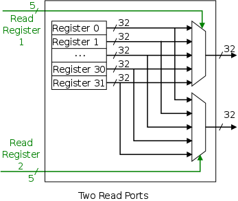
Reading From a Register File
To support reading a register we just need a (big) mux from the
register file to select the correct register.
Use one big mux for each read port.
A big
mux means an n-input, b-bit mux, where
- n is the number of registers (32 for MIPS)
- b is the width of each register (32 for MIPS)
As always we need ceiling(log(n)) bits for selecting which of the
n input to produce.
Note that we don't need two copies of the registers in order
to produce two results at the same time.
Every register is always
producing output.
All we need do is choose which 2 among the 32 results always
being produced we want to select.
Writing a Register in a Register File
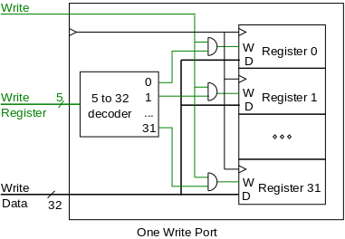
To support writing a register we use a decoder on the register
number to determine which register to write.
- The decoder is log n to n (5 to 32 for MIPS).
- The decoder outputs are numbered 0 to n-1 (NOT n).
Note that I show the clock explicitly.
Recall that the inputs to a register are W, the write line, D the
data to write (if the write line is asserted), and the clock.
We perform a write to register r this cycle if the write line is
asserted and the register number specified is r.
The idea is to gate the write line with the output of the
decoder.
- The clock to each register is simply the clock input to the
register file.
- The data to each register is simply the write data to the
register file.
- The write line to each register is unique.
- The register number is fed to a decoder.
- The rth output of the decoder is asserted if r is the
specified register.
- Hence we wish to write register r if
- The write line to the register file is asserted
- The rth output of the decoder is asserted
- Bingo! We just need an AND gate.
- We really should use the improved register or active low
register to have the full cycle to determine write.
Homework: B.36
Specifying Sequential Logic in Verilog
B.9 Memory Elements: SRAMS and DRAMS
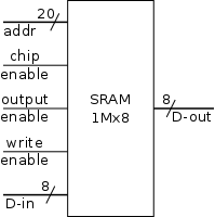
SRAM
External interface is on right.
(Sadly) we will not look inside officially.
The following is unofficial
- Conceptually, an SRAM is like a register file but we can't
use the register file implementation for a large SRAM because
there would be too many wires and the muxes would be too
big.
- We use a two stage decode.
- A 1Mx8 SRAM would need a 20-1M decoder.
- Instead the SRAM is configured internally as say thirty-two
2048x128 SRAMS.
- Pass 11 of the 20 address bits through a 11-2048
decoder and use the 2048 output wires to select the
appropriate 128-bit word from each of the sub SRAMS.
Use two of the remaining bits to select eight of the sub
SRAMS (2 bits can choose one of four 8-SRAM subsets of
the 32 sub-SRAMS).
Use the remaining 7 addr bits to select the appropriate
bit from each 128-bit word.
- Tri-state buffers (drivers) are used instead of a mux.
- I was fibbing when I said that outputs are always
either 1 or 0.
- However, we will not use tristate logic; we will use
muxes.
Dram
DRAM uses a version of the above two stage decode.
- View the memory as an array.
- First select (and save in a
faster
memory) an
entire row.
- Then select and output only one (or a few) column(s).
- So can speed up access to elements in same row.
SRAM and logic
are made from similar technologies but
DRAM technology is quite different.
- So easy to merge SRAM and CPU on one chip (SRAM cache).
- Merging DRAM and CPU is more difficult but is now being
done.
Error Correction
Note: There are other kinds of
flip-flops T, J-K.
Also one could learn about excitation tables for each.
We will not cover this material (P&H doesn't either).
If interested, see Mano.
B.10: Finite State Machines (FSMs)
More precisely, we are learning about deterministic
finite state machines or deterministic finite automata (DFA).
The alternative nondeterministic finite automata (NFA) are somewhat
strange and, althought seemingly nonrealistic and of theoretical
value only, form, together with DFAs, what I call the
secret weapon
used in the first stage of a compiler (the
lexical analyzer).
We will do a different example from the one in the book (counters
instead of traffic lights).
The ideas are the same and the two generic pictures just above apply
to both examples.
Counters
A counter counts (naturally).
- The counting is done in binary.
- The circuit increments (i.e., counts) on each clock tick
(active edge).
- Actually, it increments only on those clocks ticks when
the
increment
line is asserted.
- The state is the value of the counter.
With a 1-bit counter, there are precisely two states.
- There is one output: A, the current state of the counter.
- There are two inputs: I and R, increment and reset.
- If reset is asserted at a clock tick (i.e., at the active edge
of the clock), the counter is reset to zero.
- What should we do if both R and I are
asserted at the active edge?
- Probably that
shouldn't happen
.
We will say that the reset takes precedent.
The State Transition Diagram
The figure on the right shows the state transition
diagram for A, the output of a 1-bit counter.
- The circles represent states; the arcs represent transitions
from one state to another.
The label on the arc gives the condition for the transition to
apply.
For example, in state 1, if R=1, we transition to state 0.
- At each state, there must be a transition for each possible
value of the inputs.
- As stated above, if R=I=1, we choose to set A to zero.
That is, if Reset and Increment are both asserted, we do the
Reset.
The circuit diagram.
The circuit uses one flop and a combinatorial
circuit.
- The (combinatorial) circuit is determined by the transition
diagram.
- The circuit must calculate the next value of A from the A's current
value, I, and R.
- The flop producing A is often itself called A and the D input to this
flop is then called DA.
- To fit the diagram above for FSMs, we should not draw the
overall output (A) coming from the flop (state register) but
instead from the combinational circuit (which is easy since A is
both an input to and an output from that circuit).
- Indeed, we need to distinguish between the input A and the
output A.
- Remember that the circuit is computing A = A+1 (mod 2).
Determining the combinatorial circuit
Truth Table for the
Combinatorial Circuit
| Current | | | (Next A) |
|---|
| A | I | R | DA |
|---|
|
|
| 0 | 0 | 0 | 0 |
| 1 | 0 | 0 | 1 |
| 0 | 1 | 0 | 1 |
| 1 | 1 | 0 | 0 |
| x | x | 1 | 0 |
How do we determine the combinatorial circuit?
- This circuit has three inputs, I, R, and the current A.
- It has one output, DA, which is the
desired next A.
- So we draw a truth table, as before.
It is shown on the right.
- To remind us that we are using A (on this cycle) to calculate
A (on the next cycle), I labeled the A column as
current
A and added the label Next A to the DA
column.
- The table to the right was constructed directly (method of
perspiration).
Instead one can think about the counter and realize that
DA = R' (A ⊕ I).
A 2-bit Counter.
No new ideas are needed; just more work.
- The state diagram has 4 states 00, 01, 10, 11 and transitions from one
to another.
- The circuit diagram has 2 D-flops.
Let the top (H) flop be the high-order bit and the bottom (L) flop
the low-order bit
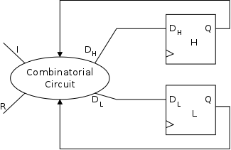
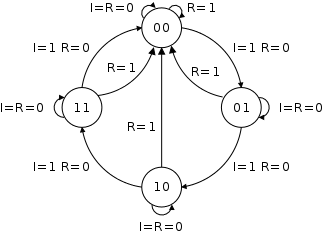
Beginning of the Truth Table for a 2-bit Counter
| Current | | |
Next |
| H | L | I | R |
DH | DL |
|
|
| x | x | x |
1 | 0 | 0 |
| 0 | 0 | 1 |
0 | 0 | 1 |
To determine the combinatorial circuit we could precede as before.
The beginning of the truth table is on the right.
This would work (do a few more rows on the board), but we can
instead think about how a counter works and see that.
  DL = R'(L ⊕ I)
  DH = R'(H ⊕ LI)
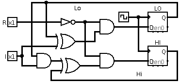
On the right is (a diagram depicting) the Logisim circuit for the
2-bit counter.
The two 1-bit registers are on the right, the clock is near the
middle and the combinatorial circuit is most of the left part.
There are two 1-bit inputs, namely I
and R.
If you want to play with this circuit the .circ file can be
downloaded here.
Run logisim and demo.
Note that I configured the logisim register to trigger on the
falling edge (our convention).
Default is to trigger on the rising edge.
A 3-bit Counter
Homework: B.39
B.11 Timing Methodologies
B.12 Field Programmable Devices
Simulating Combinatorial Circuits at the Gate Level
The idea is, given a circuit diagram, write a program that behaves
the way the circuit does.
This means more than getting the same answer.
The program is to work the way the circuit does.
For each logic box, you write a procedure with the following
properties.
- A parameters is defined for each input and output wire.
- A (local) variable is defined for each internal wire.
Really means a variable define for each signal. If a signal is
sent from one gate to say 3 others, you might not call all those
connections one wire, but it is one signal and is represented by
one variable
- The only operations used are AND OR XOR NOT
- In C or Java & | ^ !
- Other languages similar.
- Java is particularly well suited since it has variables and
constants of type Boolean.
- An assignment statement (with an operator) corresponds to a
gate.
For example A = B & C; would mean that there is an AND
gate with input wires B and C and output wire A.
- NO conditional assignment.
- NO if then else statements.
We know how to implement a mux using ANDs, ORs, and NOTs.
- Single assignment to each variable.
Multiple assignments would correspond to a cycle or to two outputs
connected to the same wire.
- A bus (i.e., a set of signals) is represented by an array.
- Testing
- Exhaustive possible for 1-bit cases.
- Cleverness for n-bit cases (n=32, say).
Simulating a Full Adder
Remember that a full adder has three inputs and two outputs.
Discuss FullAdder.c or perhaps
FullAdder.java.
Simulating a 4-bit Adder
This implementation uses the full adder code above.
Discuss FourBitAdder.c or perhaps
FourBitAdder.java
Concluding Remarks
Read.
Start Lecture #10
Chapter 2: Instructions: Language of the Machine
2.1 Introduction
Homework:
Read section 2.1.
2.2 Operations of the Computer Hardware
Homework:
Read section 2.2.
For this course you do not have to worry much about
how a program in C is translated into assembly language.
However, it is an important concept (at least at the high level).
Were this a 2-semester course, we would certainly cover it.
2.3 Operands in the Computer Hardware
Registers
Many of the MIPS instructions operate on values stored in
registers.
The MIPS architecture we shall study has thirty-two 32-bit
registers.
There is another MIPS architecture that has thirty-two 64-bit
registers.
A very serious task for a compiler (and a compiler course) is to
make efficient use of this precious resource.
Register Names
The text, which emphasizes the correspondence between a C or Java
program and assembly language much more that we shall, is very
careful in distinguishing between those registers used for C-program
variables, those used for temporary values, those used when one
function calls another, and those used for other purposes.
The hardware makes no such distinction: In machine
instructions a register operand is simply a 5-bit number (from 0 to
31).
The distinction between register types
is just a convention
used by software.
Memory Operands
Of course computers can contain many more than thirty-two 32-bit
values.
Indeed, today even a modest laptop has a central memory at least
ten million times larger.
In MIPS arithmetic is performed only on values located in
registers.
Thus, in addition to arithmetic instructions, MIPS (and essentially
all other computers) need data transfer instructions to
fetch values from memory to registers and to update memory with
newly calculated values.
The primary MIPS instructions for transferring data between
registers and memory are load-word and store-word,
written lw and sw.
Each of these instructions specifies one register and one memory
location, a.k.a. one memory address, or simply address.
In lw and sw the address consists of a
constant (a non-negative integer) and a register.
The address referenced is the sum of the constant and the contents
of the specified register.
Constant or Immediate Operands
Often one operand in an arithmetic instruction is a constant, not a
variable.
MIPS supplies corresponding immediate
instructions.
For example, the add instruction adds the contents of two
registers, placing the result in a third; whereas
the addi (add immediate) instruction adds a constant
(contained in the instruction itself) to one register, placing the
result in a second register.
2.4: Signed and Unsigned Numbers
MIPS uses 2s complement representation for signed numbers (as do
all modern processors).
As we have seen, forming the 2s complement (of 0000 1111 0000 1010
0000 0000 1111 1100) is two step procedure
- Take the 1s complement.
- That is, complement each bit (1111 0000 1111 0101 1111 1111
0000 0011)
- Then add 1 (1111 0000 1111 0101 1111 1111 0000 0100)
Unsigned Numbers
MIPS (like most computers) can also process 32-bit values as
unsigned numbers, in which case the hob is not a
sign bit.
It is instead the bit in the 231 place
As mentioned previously, addition/subtraction on signed numbers
does not treat the sign bit specially so unsigned and signed
addition/subtraction give the same answer if the operands are the
same bit strings.
The differences are in overflow and comparisons.
- For unisgned arithmetic, an overflow occurs if there is a carry
out of the hob.
- For signed arithmetic, an overflow occurs if the carry out of
the hob does not equal the carry into the hob.
- For signed values a leading 1 is smaller (negative) than a
leading 0
- For unsigned values a leading 1 is larger than a leading 0
Comments on Two's Complement
You could reasonably ask what does this funny notation have to do
with negative numbers.
Let me make a few comments.
Question: What does -1 mean?
Answer: It is the unique number that, when added
to 1, gives zero.
Our representation of -1 does do this (using regular binary
addition and discarding the final carry-out) so we do have -1
correct.
Question: What does negative n
mean, for n>0?
Answer: It is the unique number that, when
added to n, gives zero.
The 1s complement of n when added to n gives
all 1s, which is -1.
Thus the 2s complement, which is one larger, will give zero, as
desired.
Homework::
Consider the following two two's-complement binary numbers
    1010 1101 0001 0000 0000 0000 0000 0010
    1111 1111 1111 1111 1011 0011 0101 0011
What base 10 numbers does each represent?
Homework:
Consider the following base 10 numbers
2147483647 1000
Convert each to two's-complement binary.
Convert the negative of each to two's-complement binary.
2.5 Representing Instructions in the Computer (MIPS)
Hexadecimal (i.e., Base 16) Numbers
Converting base 2 values to/from base 10 is work, but converting
base 2 to/from base 16 is easy.
You simply group the base 2 number into groups of 4 or expand the
base 16 number from right to left.
The one question is how do you write the 6 digits past 9 and the
answer is A, B, C, D, E, and F.
Do some examples on the board.
The Register File
We just learned how to build this structure.
We need 2 read ports and 1 write port since MIPS instructions can
read up to 2 register and write up to 1 register.
We shall follow convention, and denote the 32 registers as $0, $1,
..., $31.
As mentioned previously, the book, more than the course, emphasizes
how high-level instructions are translated into MIPS instructions.
As a result the book uses a more sophisticated naming scheme for
registers with two characters after the dollar sign.
The first character is a letter and indicates what the software
conventionally uses the register for.
For example $t2 is the third ($t0 is the
first) register used for temporary values.
As stated above, MIPS has thirty-two 32-bit register.
Some machines, notably the 32-bit Intel (PC) architecture, have a
number of register classes, where only certain registers can be used
for certain task.
However, the MIPS treats registers 1-31 the same, only register 0 is
special.
- Register 0 gives 0 when read.
- Stores to register 0 are ignored.
MIPS Fields
The fields of a MIPS instruction are fairly consistent.
There are just a few classes of instruction formats and within each
class the various bit positions of the instructions are used in the
same way.
R-type Instructions (R for Register)
These instructions have three operands, each is a register number.
All R-type instructions have the following fixed format.
  op    rs    rt    rd    shamt  funct   name of field
   6     5     5     5      5      6     number of bits
These fields are used consistently in R-type instructions.
- op is the opcode
- rs,rt are source operands
- rd is destination
- shamt is the shift amount
- funct is used for op=0 to distinguish alu operations add, sub,
and, or, etc.
- Try not to be confused by the fact that in the machine
instruction the destination is the last register specified, but
in the assembler examples below the destination is first.
Add and Subtract op rd,rs,rt
Examples: add/sub $9,$10,$11).
- Register 9 becomes register 10 +/- register 11.
- R-type instructions use the format above.
- The first example given (add) has for its 6 fields
0—10—11—9—0—32
- op=0, signifying an alu op.
- The shamt is not used (set to zero).
- funct=32 specifies add.
Funct determines the control bits to the alu.
- All three register numbers can be the same (for add this doubles
the value in the register).
- Do sub by just changing the funct.
- Note that, if the three register numbers are the same for
subtract, the effect is to clear (i.e., set to zero) the
register.
I-type (Immediate)
The I is for immediate.
Load Word and Store Word op rt, immediate(rs)
Examples: lw/sw $9,1000($19)
- The constant 1000 is the immediate operand.
- The effect of the lw example is that register $9 is
loaded with the contents of Mem[$19+1000] (i.e., with the contents
of the memory location whose address is formed by adding 1000 to
the contents of register $19).
The contents of memory is unchanged.
The contents of register $19 unchanged.
- The effect of the sw example is that Mem[$19+1000] is
changed to have the value currently in register $9.
The contents of both registers are unchanged.
- The format of the lw example is 35-19-9-1000
- The format of the sw is the same with opcode 43.
Add Immediate op rt, rs, immediate
Example: addi $9,$10,100
- The effect of the instruction is
$9 = $10 + 100
- The opcode for addi is 8
- The format of the example is
8—10—9—100 .
Question: Why is there no subi?
Answer: The immediate operand in addi
can be negative.
Homework:
Consider the following MIPS assembly instructions
    addi $1,$1,-20
    add  $1,$1,$2
    lw   $3,8($1)
Assume initially $1 contains 256, $2 contains 20 and that memory
contains
    addr     value
    256      100
    260      200
    264      300
What is the final value of $3?
Homework:
Consider the following 32-bit binary numbers
    1010 1110 0000 1011 0000 0000 0000 0100
    1000 1101 0000 1000 0000 0000 0100 0000
What instructions do they represent (write the answer in MIPS
assembler)?
Is each an R-type or I-type instruction.
Homework:
Consider
    add $4,$4,$0
    lw  $5,4($3)
Write the binary for these instructions and give the type (R or I)
for each.
2.6: Logical Operations
These instructions deal with the bits within the word rather than
treating the word as a unit.
Such instructions are often called logical
.
Left and Right Shift
Shift Left/Right Logical op rd, rt, shamt
Examples: sll/srl $15,$10,7
- These examples set register 15 to the value obtained by
shifting the contents of register 10 left/right 7 bits and
setting the 7 rightmost/leftmost bits to 0.
Register 10 is not changed.
- Naturally the two register numbers can be the same.
- This is an R-type instruction, with shamt used and
rs not used.
- The op is 0.
- The funct is 0/2 for sll/srl.
- The format of the sll example is
0—0—10—15—7—0.
The srl example is the same except the last field
(funct) is 2.
- Question: Why do we need both sll
and srl, i.e, why not just have one of them and use a
negative shift amt for the other?
Answer: The shamt is only 5 bits and
we need shifts from 0 to 31 bits.
Hence not enough bits for negative shifts.
- Question: Why do we need shifts up to 31 bits?
Isn't a left shift by 26 bits the same as a right shift by 32-26=6
bits?
Answer: NO!
These are shifts not rotates.
Boolean Ops: AND, OR, and NOR
(Bitwise) AND, OR, and NOR op rd, rs, rt
Examples: and/or/nor $18,$17,$16
- Three R-type instructions.
- The operations are performed bit by bit as we did in our
alu.
- The op is zero.
- The shamt is not used (always 0).
- The funct is 32 for AND, 35 for OR and 39 for
NOR.
- The format of the AND example is
0—17—16—18—0—32
- The OR and NOR examples are the same except for
the funct field.
- NOT is a special case of NOR: NOT X = X NOR FALSE and register
$0 is always 0.
Hence, for example, nor $9,$9,$0 simply negates
each bit of register 9.
Note that this is the same as taking the one's compliment.
Immediate Versions op rt, rs, immediate
Examples andi/ori 16,8,31
- I-type instructions.
- The op is 12/13.
- The format of the andi example is
12—8—16—31.
- The ori example has the same except for
the op.
- The instruction nori was not considered useful enough
to warrant an additional opcode.
Homework:
Assume
$r1=0101 0101 0101 0101 0101 0101 1010 1010
and
$r2=0001 0010 0011 0100 0101 0110 0110 1000
What is the value of $3 for the following sequence of instructions?
    sll $3, $1, 4
    or  $3, $3, $2
What is the value of $3 for the following sequence of instructions?
    sll  $3, $1, 4
    andi $3, $3, -1
Start Lecture #11
2.7 Instructions for Making Decisions
Conditional Branches
Branch (Not) Equal op rt, rs, immediate
Examples: beq/bne $9,$10,123
- I-type instruction.
- The beq example means:
if reg-9==reg-10 then go to the 124rd instruction after this
one
.
- The bne example means:
if reg-9!=reg-10 then go to the 124rd instruction after this
one
.
- Question: Why 124 not 123?
Answer: Branching to the 0th instruction after
this one is worse than useless (it is an infinite loop).
- The op is 4/5
for beq/bne.
- The format of the beq example is
4—10—9—123.
The bne example has the same format except for
the op.
- Normally one writes a label for the third
operand and the assembler calculates the offset needed.
Two's Complement Comparisons
Set Less Than op rd, rs, rt
Example: slt $9,$10,$11
- This is an old friend.
- Recall the extra effort we put into the alu a few weeks ago to
implement this important MIPS instruction.
- An R-type instruction.
- Set register-9 to
if register-10 < register-11 then 1 else 0
- The op is 0.
- The shamt is ignored (always 0).
- The funct is 42.
- The format of the example is
0—10—11—9—0—42.
Set Less Then Immediate op rt, rs,
immediate
Example: slti 17,18,20000
- I-type instruction.
- Set register-17 to (if register-18 < 20000 then 1 else 0).
- The op is 10.
- The format of the example is
10—18—17—20000.
Unsigned Comparisons
Recall that comparison is different for unsigned and signed
numbers: Signed values with 1 in the hob are less than those with 0
in the hob (the first value is negative); but, if the values are
unsigned, a 1 in the hob is greater than a 0 in the hob.
For this reason, MIPS has in addition to the above, unsigned
versions of slt and slti, that use the
unsigned definition of less than.
The instructions are named sltu and sltiu as
you would expect.
Our MIPS subset implementation, will not include them.
Additional Comparisons and Conditional Branches
Branch Less Than
Example: blt $13,$15,123
- I-type
- if $13 < $15 then go to the 124rd instruction after this one.
- *** WRONG ***
- There is no blt instruction.
- Instead use
        stl $1,$13,$15

        bne $1,$0,123
Branch Less Than Or Equal and Set Than or Equal
Examples: ble $5,$7,123 and
sle $1,$5,$7
- Wrong!
- There is no
ble $5,$7,123
instruction.
- There is also no
sle $1,$5,$7
, set $1 if $5 less
or equal $7.
- Note that $5 ≤ $7 is the same as NOT ($7 < $5).
- Hence we test for $7 < $5 and branch if false.
        stl $1,$7,$5

        beq $1,$0,L
Branch Greater Than and Set Greater Than
Examples: bgt $5,$7,123 and
sgt $1,$5,$7
- Wrong!
- There is no
bgt $5,$7,123
instruction.
- There is also no
sgt $1,$5,$7
, set $1 if $5
greater than $7.
- Note that $5 > $7 is the same as $7 < $5.
- Hence we test for $7 < $5 and branch if true.
        stl $1,$7,$5

        bne $1,$0,L
Branch Greater Than Or Equal and Set Greater Than or Equal
Examples: bge $5,$7,Land
sge $1,$5,$7
- Wrong!
- There is no
bge $5,$7,123
instruction.
- There is also no
sge $1,$5,$7
, set $1 if $5 greater or
equal $7.
- Note that $5 ≥ $7 is the same as NOT ($5 < $7).
- Hence we test for $5 < $7 and branch if false.
        stl $1,$5,$7

        beq $1,$0,L
Note:
Please do not make the mistake of thinking that
        stl $1,$5,$7

        beq $1,$0,L
is the same as
        stl $1,$7,$5

        bne $1,$0,L
It is not true that the negation of X<Y
is Y>X.
End of Note
J-type instructions (J for jump)
These have a different format from R-type and I-type instructions,
but, as always, the opcode is the first 6 bits and determines the
format.
    op   address
    6    26
The effect is to jump to the specified (immediate) address.
Note that there are no registers specified in this instruction
and that the target address is not relative to
(i.e. added to) the address of the current instruction as was done with
branches.
Simple Jumps
Jump op address
Example: j 10000
- A J-type instruction.
- Jump to instruction (not byte) 10000.
- As we have sceen, branches are PC relative, jumps, however, are
absolute.
- Range is 226 words = 228 bytes =
1/4 GB
- The op is 2.
- The format of the example is 2—10000.
But MIPS is a 32-bit machine with 32-bit address and we have
specified only 26 bits.
What about the other 6 bits?
In detail the address of the next instruction is calculated via a
multi-step process.
- The 26 bit address field is extracted from the instruction.
- This address is left shifted two bits.
The result is a 28-bit address (call it A) that is always a
multiple of 4, which makes sense since all instructions must
begin on a multiple of 4 bytes.
- The high order 4 bits are extracted from the
address of the current instruction
(not the address in the
current instruction).
Call this 4-bit quantity B.
- The address of the next instruction is formed by concatenating
B with A.
Homework: Consider the
following possible values for $1
    1010 1101 0001 0000 0000 0000 0000 0010
    1111 1111 1111 1111 1111 1111 1111 1111
suppose $2 contains
0011 1111 1111 1000 0000 0000 0000 0000
For each $1 what is the value of $3 after
executing
slt $3, $1, $2
2.8 Supporting Procedures in Computer Hardware
Calling a Procedure and Returning from It
Jump And Link op address
Example: jal 40000
- A J-type instruction.
- Jump to instruction (not byte) 40000 and store the return
address (the address of the instruction after the jal)
in register 31 (by convention often called ra).
- The op is 3.
- The format of the example is 3—40000
- By using a fixed register (register-31 in this
case), jal avoids the need for a second register
field and hence can have 26 bits for the instruction address
(i.e., can be a J-type instruction).
- Used for subroutine calls.
The value stored in $ra is the address the called
routine must jump to when it want to return to its caller.
Jump Register op rs
Important example: jr $31
- An R-type instruction, but uses only one register
rs.
- Jump to the location in the specified register.
- The important example is used to return from a subroutine called
via a jal.
- The op is 0 and the funct is 8.
- The rt, rd, and shamt fields
are not used.
- The format of the example is
0—31—0—0—0—8.
2.9 Communicating with People
2.10 MIPS Addressing for 32-bit Immediates and Addresses
How can we put a 32-bit value (say 2 billion) into register 6?
- Zero and add.
- Zero register 6 with sub $6,$6,$6
- then add 2 billion with
addi $6,$6,2000000000.
- WRONG: 2 billion doesn't fit in the 16-bit
immediate field of an addi.
- Load the word
- Have the constant placed in the program text (via some
assembler directive).
- Issue lw to load the register.
- This works
- It is inefficient since memory accesses are slow (and the
load uses a cache entry).
- Load shift add
- First decompose 2,000,000,000 into its high order 16 bits
and its low order 16 bit.
- 2^16 = 65,536
- The high order 16 bits is 2,000,000,000 / 65,536 =
30,517 and the low order is 2,000,000,000 % 65,536 =
37888.
- Load immediate the high order 16 bits (into the low order
bits of register 6).
This uses the lhi (load halfword immediate)
instruction that we haven't learned:
lhi $6,30517.
- Shift register 6 left 16 bits (filling the low order with
zero): sll $6,$6,16.
- Add immediate the low order 16 bits to register 6.
addi $6,$6,37888.
- Watch out!
The add immediate might actually subtract!
Why, how?
If the immediate value has the hob set, it is negative.
- Load shift OR
- Load immediate the high order 16 bits (into the low order
bits of register 6):
lhi $6,30517.
- Shift register 6 left 16 bits (filling the low order with
zero): sll $6,$6,16.
- OR immediate the low order 16 bits to register 6:
ori $6,$6,37888.
- This works.
- But it uses three instructions.
Can we do better?
A Combined Load and Shift
Load Upper Immediate op rt, immediate
Example: lui $12,123
2.11 Parallelism and Instructions: Synchronization
2.12 Translating and Starting a Program
2.13 A C sort Example to Put it All Together
2.14 Arrays versus Pointers
2.15 Advanced material: Compiling C and Interpreting Java
2.16 Real Stuff: ARMv7 (32-bit) Instructions
2.17 Real Stuff: x86 Instructions
2.18 Real Stuff: ARMv8 (64-bit) Instructions
2.19 Fallacies and Pitfalls
2.20 Concluding Remarks
2.21 Historical Perspective and Further Reading
Chapter 3: Arithmetic for Computers
Homework: Read 3.1-3-4
3.1 Introduction
I have nothing to add.
3.2 Addition and Subtraction
Recall that MIPS uses 2s complement (just like the intel chips)
To form the 2s complement (of 0000 1111 0000 1010 0000 0000 1111 1100)
- Take the 1s complement.
- That is, complement each bit (1111 0000 1111 0101 1111 1111
0000 0011)
- Then add 1 (1111 0000 1111 0101 1111 1111 0000 0100)
To add two (2s complement) numbers just add them.
That is, don't treat the sign bit special.
To subtract A-B, just take the 2s complement of B (forming -B) and
add.
Overflows
An overflow occurs when the result of an operation cannot be
represented with the available hardware.
For MIPS this means when the result does not fit in a 32-bit word.
Recall that the operands each have 31 data bits and a sign bit;
thus the result would definitely fit in 33 bits (32 data plus 1
sign).
  11111111111111111111111111111111   (32 ones is -1)
+ 11111111111111111111111111111111
----------------------------------
 111111111111111111111111111111110   Discard the carry out
  11111111111111111111111111111110   this is -2 as desired
As shown on the right the hardware simply discards the carry out of
the high order (i.e., sign) bit, which might seem hopelessly naive,
but is normally correct.
The bottom 31 bits are always correct.
Overflow occurs when the 32nd (sign) bit is set to a value and not
the sign.
An overflow cannot occur when adding numbers with
different signs or when subtracting numbers with the same sign.
Specifically, an overflow occurs in the following cases
  Operation  Operand A  Operand B  Result
  A+B         ≥ 0          ≥ 0       < 0
  A+B         < 0          < 0       ≥ 0
  A-B         ≥ 0          < 0       < 0
  A-B         < 0          ≥ 0       ≥ 0
These conditions are the same as
Carry-In to sign position != Carry-Out from sign position.
Homework:
Prove this last statement (for fun only, do not hand in).
addu, subu, addiu
Since unsigned numbers are often used for address arithmetic where
overflows should be ignored, these three instructions perform
addition and subtraction the same way as do add and
sub, but do not signal overflow.
3.3 Multiplication
Of course we can do this with two levels of logic since
multiplication is just a function of its inputs.
But just as with addition, would have a very big circuit and
large fan in.
Instead we use a sequential circuit that mimics the algorithm we
all learned in grade school.
Recall how you learned to multiply in the fifth grade.
- Terminology: Multiplicand times multiplier gives product.
- Multiply multiplicand by each digit of multiplier.
- Put the result in the correct column.
- Then add the partial products just produced.
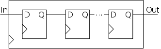
Shifter
This is a sequential circuit.
I don't believe it is in the text, but we need it for
multiplication.
The simplest shifter is just a string of D-flops; the output of one
is input of the next.
- Input to first is the serial input.
- Output of last is the serial output.
We want more.
- Bidirectional, i.e., left and right shifting (with serial
input/output).
- Parallel load.
- Parallel Output.
- Don't shift every cycle.
Parallel output is just wires.
The shifter on the right always produces the Out[1:3] lines, giving
the current value of the 3 flops.
It has 4 modes of operation depending on the 2-bit OP control lines.
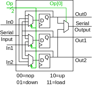
- Nop.
- The serial input is ignored and the serial output is undefined.
- The 3-bit register (i.e., the flops) is unchanged.
- Shift down.
- The serial output is the previous value of the bottom
flop.
- The bottom flop becomes the previous value of the middle
flop.
- The middle flop becomes the previous value of the top
flop.
- The top flop becomes the value of the serial input at the
active edge.
- Shift up.
- The serial output is the previous value of the top flop.
- The top flop becomes the previous value of the middle flop.
- The middle flop becomes the previous value of the top flop.
- The bottom flop becomes the value of the serial input at the
active edge.
- Load.
- The serial output is undefined.
- The top flop becomes the value of In0 at the active edge.
- The middle flop becomes the value of In1 at the active edge.
- The bottom flop becomes the value of In2 at the active edge.
Since there are four modes we are not surprised to see.
- A 4-input mux feeding each flop.
- Two external control lines for the muxes.
We could modify our registers to be shifters as well (bigger mux),
but ...
These shifters are slow for big shifts; barrel shifters
are
faster and kept separate from the processor registers.
Homework: A 4-bit shift
register initially contains 1101. It is shifted six times to the
right with the serial input being 101101.
What is the contents of the register after each shift.
Homework: Same
register, same initial condition.
For the first 6 cycles the opcodes are left, left, right, nop, left,
right and the serial input is 101101.
The next cycle the register is loaded (in parallel) with 1011.
The final 6 cycles are the same as the first 6.
What is the contents of the register after each cycle?
Start Lecture #12
Remarks.
- Practice midterm on classes (resources).
- Covers through this chapter, which we will finish today.
- Real midterm on 24th or 26.
- Let's vote.
- Little or no office hour on 24th.
- Can have extended 12-1:30 on 26th.
The First Attempt at a Multiplier
Our first solution multiplies in essentially the
same way as we do by hand.
We are doing binary arithmetic so each digit
of the
multiplier is 1 or zero.
Hence multiplying
the mulitplicand by a digit of the
multiplier results in either
- Getting the multiplicand
- Getting zero
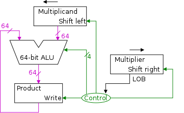
Use an if appropriate bit of multiplier is 1
test.
To get the appropriate bit
:
- Start with the LOB of the multiplier
- Shift the multiplier right (so the next bit is the LOB)
Putting it in the correct column means putting it one column
further left than the last time.
This is done by shifting the multiplicand left one bit each
time (even if the multiplier bit is zero).
Instead of adding the partial products at end, we keep a running
sum.
- If the multiplier bit is one, add the (shifted)
multiplicand to the running sum.
- If the bit is zero, simply skip the addition.
This results in the following algorithm
    product ← 0
    for i = 0 to 31
        if LOB of multiplier = 1
            product = product + multiplicand
        shift multiplicand left 1 bit
        shift multiplier right 1 bit
What about the control?
- Always give the ALU the ADD operation (easy; it's a
constant!).
- Always send a 1 to the multiplicand to shift left (easy; another
constant!).
- Always send a 1 to the multiplier to shift right(easy;
constant!).
- Pretty boring so far but what about the write line, which is
not constant.
- Send a 1 to the write line in product if and only if
the LOB of the multiplier is a 1.
- That is, send LOB to write line.
- So the control really is pretty boring.
- Reading CW from the bottom left the output of control is
(LOB, ADD, 1, 1) and LOB is also an input to the
control.
This works!
It clearly works if we test the LOB and write the
product on one cycle and shift the next cycle (so two cycles per bit).
With some more care you can do it all in one cycle, you just need
to be sure you add the multiplicand before it is shifted and that
you get the LOB before the multiplier is shifted.
Do on the board 4-bit multiplication (using 8-bit registers for
multiplicand, and product) 1100 x 1101.
Since the result has (up to) 8 bits, this is often called a 4x4→8
multiply.
The diagrams are for a 32x32→64 multiplier.
The weakness of the above solution, when compared to the improved
versions to come, is that the first attempt is wasteful of resources.
and hence is:
- slower
- hotter (and therefore uses more energy)
- bigger
All these are bad.
An Improved Circuit
We question why all the circuitry must be 64-bits
wide.
Question: Why is the product register 64-bits
wide?
Answer: Because the product can contain 64
bits.
Question: Why is multiplicand register 64 bits?
Answer: So that we can shift it left, i.e., for our
convenience.
By this I mean it is not required by the problem specification,
but only by the solution method chosen.
Question: Why is ALU 64-bits?
Answer: Because the product which is one of the
inputs can contain 64-bits.
- But we are only adding a 32-bit quantity to the product at any
one step.
- Hmmm.
- Maybe we can just pull out the correct bits from the product.
- It seems hopeless because which bits to pull changes each
step.
- POOF!!
... as the smoke clears we see an idea.
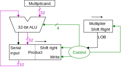
We can solve both problems at once.
Don't shift the multiplicand left
- Hence the multiplicand register is only 32-bits, solving problem 1.
- Also this register need not be a shifter.
Instead shift the product right!
Add the high-order (HO) 32-bits of product register to the
multiplicand and place the result back into HO 32-bits
- Only do this if the current multiplier bit is one.
- Use the Carry Out of the sum as the new bit to shift in.
That is, the algorithm becomes
  product = 0
  for i = 0 to 31
      if LOB of multiplier = 1
         (serial_in, product[32-63]) = product[32-63] + multiplicand
      shift product right 1 bit
      shift multiplier right 1 bit
What about control?
- Just as boring as before.
- Again reading CW from the bottom left we send
(LOB, 1, ADD, 1) to
(Product (write), Product (shift right), ALU, multiplier
(shift right)).
Redo the same example on the board.
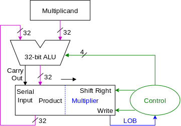
A final trick
There is a still waste of registers, i.e. they are
not fully utilized.
- The multiplicand is fully unilized since we always need all
32 bits.
- But once we use a multiplier bit, we can toss it so we need
less and less of the multiplier as we go along.
- And the product is half unused at beginning and only
slowly ...
- Another POOF!!
Timeshare
the LO half of the product register
.
- In the beginning LO half contains the multiplier.
- Each step we shift right and more of the register goes to
the product, less to the multiplier.
The algorithm changes to:
    product[0-31] ← multiplier
    for i = 0 to 31
        if LOB of product = 1
            (serial_in, product[32-63]) ← product[32-63] + multiplicand
        shift product right 1 bit
Control again boring.
- Send (ADD, 1) to (ALU, Product (shift right)).
- Send LOB to Product (write).
Redo the same example on the board.
Signed Multiplication
The above was for unsigned 32-bit multiplication.
What about signed multiplication?
- Save the signs of the multiplier and multiplicand.
- Convert multiplier and multiplicand to non-negative numbers.
- Use above algorithm on the non-negative numbers.
- Only use 31 steps not 32 since there are only 31 multiplier bits
(the HOB of the multiplier is the sign bit, not a bit used for
multiplying).
- Compliment the final product if original signs were
different.
Faster Multipliers
There are (asymptotically) faster multipliers, but
we are not covering them.
3.4 Division
3.5 Floating Point
3.6 Parallelism and Computer Arithmetic: Associativity
3.7 Real Stuff: Floating Point in the IA-32
3.8 Fallacies and Pitfalls
Read for pleasure.
3.9 Concluding Remarks
Read for pleasure.
3.10 Historical Perspectives
Read for pleasure (located on CD).
Note: End of material on midterm.
I will post a practice midterm and later solutions.
Advice: do NOT look at the answers until you have
done the questions.
Chapter 4 The Processor
Homework: Start Reading
Chapter 4.
4.1: Introduction
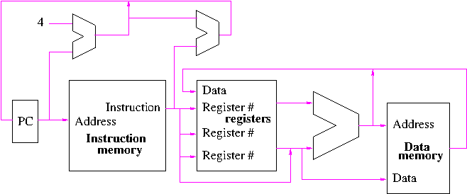
We are going to build
a basic MIPS processor.
Figure 4.1 redrawn below shows the main idea.
Note that the diagram shows the instruction including three
register numbers, an immediate value to be added to a register, and
an immediate value to be added to the PC.
No single instruction has all those components, but our datapath
must include pathways for all possibilities.
Eventually, we will add muxes to choose which possibilities are
relevant for the given instruction.
We shall see how we arrange for only certain datapaths to be used
for each instruction type.
- For example, R-type instructions uses all three registers but
not the immediate field.
- I-type instructions use the immediate but only two registers.
- The memory address for a load or store is the sum of a register
and an immediate.
- The data value to be stored comes from a register.
Question: Why are we doing arithmetic on the
program counter?
Answer: The first adder is to move to the next
sequential instruction.
The second adder is to deal with branches (not jumps) since they are
PC-realative.
4.2 Logic Design Convention
Done in appendix B.
4.3 Building a Datapath
Let's begin doing the pieces in more detail.
We draw buses in magenta (mostly 32 bits) and control lines in
green.
Instruction Fetch
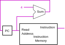
We are ignoring branches and jumps for now.
The diagram on the right shows the main loop
involving
instruction fetch (i-fetch)
- Question: How come no write line for the PC
register?
Answer: We write it every cycle.
- Question: How come no write line for the
instruction memory.
Answer: We never write it (of course somehow it
is written).
- Question: How come no control for the ALU?
Answer: This one always adds.
- Question: How come no clock lines.
Answer: Lazy; they should be drawn.
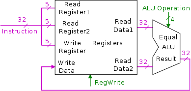
R-type instructions
We did the register file in appendix B.
Recall the following points made when discussing the appendix.
- The words
Read
and Write
in the diagram are
adjectives not verbs.
- The register file contains two read ports and one write port.
We mentioned in the appendix that this was to support MIPS
instructions that read two and write one register.
Now that we have covered the basic MIPs instructions, we know that
it is R-type instructions that have this requirement.
- The 4-bit control line sent to the ALU consists of ANegate,
BNegate, and the 2-bit Operation.
- We learned that the RegWrite control line is asserted if
the Write Register is to be written.
The 32-bit bus with the instruction is divided into three 5-bit
buses, one for each register number (plus 17 other wires not
shown).
Homework: What would happen to R-type
instructions, if the RegWrite line had a stuck-at-0 fault (was
always deasserted)?
What would happen if the RegWrite line had a stuck-at-1 fault (was
always asserted)?
Notation for Register Numbers
In this chapter we are interested in building the processor, and not
as interested in seeing how Java or C statements could be
translated into machine instructions.
As a result, I will refer to the registers in an instruction by
their hardware names
- rs (always a source register) is specified in bits 25-21 of the
instruction.
- rt (sometimes a source and sometimes a destination) bits
20-16.
- rd (always a destination) bits 15-11.
Start Lecture #13
Remark: Midterm on 26 September.
Load and Store
The diagram on the right shows the structures used to implement
load word and store word (lw and sw).
The book includes a MemRead control line.
We simplify the presentation by assuming RAM is like registers and
always supplies output on ReadData.
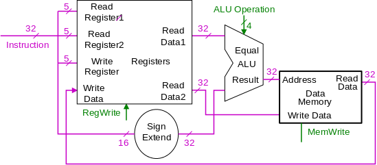
lw rt,disp(rs):
- Computes the effective address formed by adding the 16-bit
immediate constant
disp
(displacement) to the contents of
register rs.
- Fetches the value in data memory at this address.
- Writes this value into register rt.
- rd is not used.
Those 5 bits are part of the 16-bit immediate field.
sw rt,disp(rs):
- Computes the same effective address as lw rt,disp(rs).
- Stores the contents of register rt into this address.
- Again rd is part of the immediate field so is not used.
Sign Extension
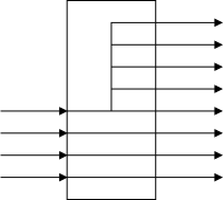
We have a 32-bit adder and have a 32-bit addend
coming from the register file.
Hence we need to extend the 16-bit immediate constant to 32 bits.
That is we must replicate the HOB of the 16-bit immediate constant
to produce an additional 16 HOBs all equal to the sign bit of the
16-bit immediate constant.
This is called sign extending the constant.
Note that the Sign Extend oval consists of just wires, no gates at
all.
On the right is a small example, a 4→8 sign extender.
Control Lines
What about the control lines?
- RegWrite is deasserted for sw and asserted for lw.
- MemWrite is asserted for sw and deasserted for lw.
- We don't have MemRead since our memory (unlike Ram in a real
machine) is the same as our registers.
- The ALU Operation is set to
add
for both lw and sw.
- For now we just write down which control lines are asserted and
deasserted.
Later we will do the circuit to calculate the control lines given
the instruction word.
Homework: What would
happen to lw/sw if the RegWrite line had a stuck-at-0 fault (was
always deasserted)?
What would happen if the RegWrite line had a stuck-at-1 fault (was
always asserted)?
What would happen if the MemWrite line had a stuck-at-0 fault?
What would happen if the MemWrite line had a stuck-at-1 fault?
The Diagram is Wrong (Specifically, Incomplete)
The diagram cheats a little for clarity.
- For lw we write register rt (and read rs).
- For sw we read register rt (and read rs).
- But we indicated that the same bits in the instruction always go to
the same ports in the register file.
- We are
mux deficient
.
Problem: Some of the time we want of one group of
bits to go to a given port; other times we want another group to
go to that same port.
Solution: Always send the first group toward the
port; always send the second toward the port; and use a mux to
choose which group actually gets to the port.
- We will put in the muxes later.
Branch on Equal (beq)
Compare two registers and branch if equal.
The circuit on the right computes two values, the branch target
address and a Boolean specifying whether or not to branch.
Note the familiar pattern.
- We might branch and we
might not branch.
- We always compute the address assuming
we do branch.
- We always compute the address assuming
we don't branch.
- We compute a control signal that will goes to a mux, which
chooses between the two addresses
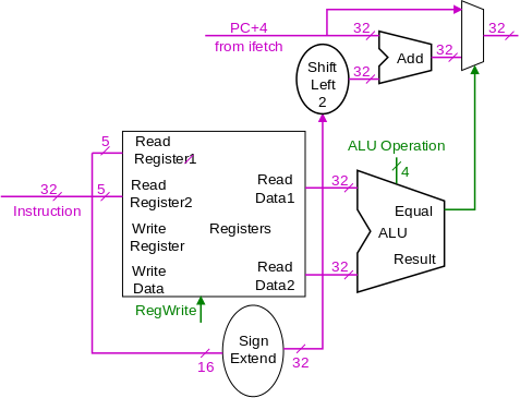
Remember that this diagram is just for beq.
If the instruction is not beq then the Equal line from the ALU is
not relevant.
This will be fixed up later when we do all the control.
Recall the following from appendix B, where we built the ALU, and
from chapter 2, where we discussed beq.
To check if two registers equal we subtract one from the other and
test the result for zero (our ALU subtracts if ALU Operation says
to, and our ALU always checks if the result is 0).
In this case we are not interested in the result itself (so we don't
wire that output to anything), just whether it is zero.
The target of the branch on equal instruction
beq rs,rt,disp
(assuming we do branch) is the sum of
- The program counter PC after it has been incremented,
that is, the address of the next sequential
instruction.
This address is always calculated by the ifetch unit above.
- The 16-bit immediate constant
disp
(treated as a signed
number) left shifted 2 bits.
The constant represents (32-bit) words and the
address is specified in (8-bit) bytes).
Since there are 4 bytes per word, we must multiple the word
address by 4, which can be accomplished by a left shift of 2.
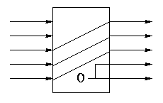
The shift left 2 is not a shifter (it has no state, i.e., no
memory).
It simply moves wires and includes two zero wires.
We need a 32-bit version of the 5 bit version shown on the
right.
Since the immediate constant is signed it must be sign extended.
As mentioned and drawn previously this is just replicating the
HOB.
The top alu labeled add
is just an adder so does not need
any control.
Homework: What would
happen to Branch on Equal if the RegWrite line had a stuck-at-0
fault?
What would happen if the RegWrite line had a stuck-at-1 fault?
Creating a Single Datapath
We will first put the pieces together in a way that the resulting
single datapath is able to execute all of the above instructions
(several R-type instructions including set-less-than, load and store
word, and branch on equal).
This will require several multiplexors and their associated select
lines.
After we have the pieces assembled into a unified whole, we will
discuss how to calculate the select lines (and other control lines).
We are not now worried about speed.
We are assuming that the instruction memory and data memory are
separate.
So we are not permitting self modifying code.
We are not showing how either memory is connected to the outside
world (i.e., we are ignoring I/O).
We must use the same register file for all the
instruction types since when a load changes a register, a subsequent
R-type instruction must see the change and when an R-type
instruction makes a change, the lw/sw must see it (for storing or
calculating the effective address).
We could use separate ALUs for each type of instruction so that
several instructions could proceed at the same time, but we are
not worried about speed so we will use the same ALU for all
instruction types.
We do have a separate adder for incrementing the PC (because it is
easier to do so).
Combining R-type and lw/sw
The problem is that some inputs can come from different sources
depending the instruction type.
We need to add muxes as shown below.
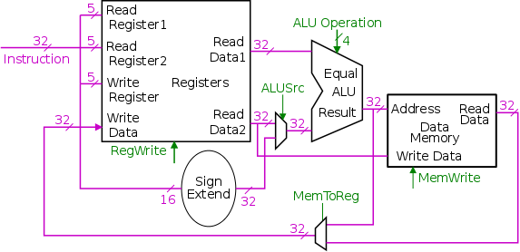
- For R-type instructions, both ALU operands are registers.
For I-type instructions (lw/sw) the second operand is the (sign
extended) immediate field.
This is handled by the mux with control line named ALUSrc.
The name was presumably chosen to indicate that this control line
determines one of the sources (i.e., inputs) for the ALU.
- For R-type instructions, the write data comes from the ALU.
For lw it comes from the memory.
See the control line MemToReg (i.e., should the value from the
Memory go to the Register).
- For R-type instructions, the write register comes from field rd,
which is bits 15-11.
For sw, the write register comes from field rt, which is bits
20-16.
The diagram does not deal with this issue.
We shall do it later using (surprise) another mux.
Including Instruction Fetch
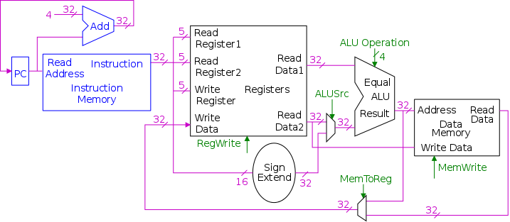
Adding instruction fetch is quite easy.
We simply attach the instruction fetch block done above to the left
of the previous diagram.
The result is shown on the right, where the new material is in
blue.
Not shown yet is how the 32-bit instruction leaving the instruction
memory is divided into into the various 5-bit and 16-bit fields.
This is not trivial since it is not true that the
same bits always go to the same place.
Including beq
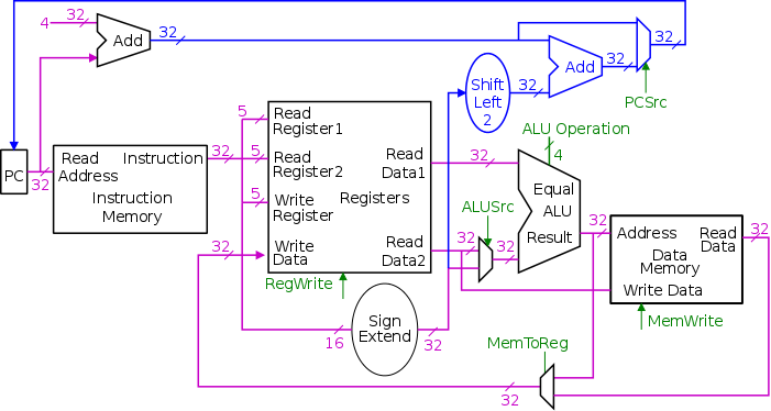
We need to have an if stmt
for updating the PC corresponding
to the two possiblities: the branch is taken and the branch is not
taken.
This conditional assignment to the PC should be compared to the
conditional expressions found in C and Java, for example
y = (c==4) ? x : z;
As usual, in logic design the conditional assignment is done with a
mux (and a control line, named PCSrc—what is the input to the
PC register).
Homework: Extend the
datapath just constructed to support the addi instruction as well as
the instructions already supported.
Homework: Extend the
datapath just constructed to support an R-type instruction that is a
variation of the lw instruction where the memory address is computed
by adding the contents of two registers (instead of using an
immediate field) and the contents of that memory location is loaded
into the third register.
Continue to support all the instructions that the original datapath
supported.
Homework: Can you
support a hypothetical swap instruction that swaps the contents of
two registers using the same building blocks that we have used to
date?
Start Lecture #14
Remark: The stuck at
duplication
explained.
4.4: A Simple Implementation Scheme
What is Left to Do?
There are basically two tasks remaining.
We shall see they are related; the key is the instruction itself.
- Dividing the Instruction.
The diagram above has a 32-bit instruction magically divided into
various fields, three of 5-bits and one of 16 bits.
Moreover we know that not all fields are relevant for all
instructions: I-type instructions do not have a third register and
R-type instructions do not have a 16-bit immediate field.
In addition, register rt is sometimes a read register and
sometimes a write register.
We must figure which bits of the 32-bit instructions should go to
each of the various fields in all possible circumstances.
- Setting the Muxes and Other Control Lines.
We have ignored the control signals.
Each of our muxes has a 1-bit control line that appears to be
created out of thin air.
We need to determine the values of each of these lines for all
cases.
Similarly, our ALU takes a 4-bit control line, but we have not
determined how to calculate those four bits.
Dividing the Instruction
The diagram below shows (in blue as usual) the additions needed to
divide the instruction.
One cost
of this solution is yet another mux, with yet
another to-be-calculated 1-bit control line (having yet another
slightly cryptic name RegDst, meaning this line determines whether
Register rt or rd should be the Destination register).
Also added is an unspecified logic block ALU Cntl
, with
an unspecified 2-bit control line ALUOp
as one of its inputs.
The new control lines will be determined in the next section
entitled The Control for the Datapath
, and the new block will
calculate the 4-bit ALU Operation from the new control lines and the
funct bits of the instruction.
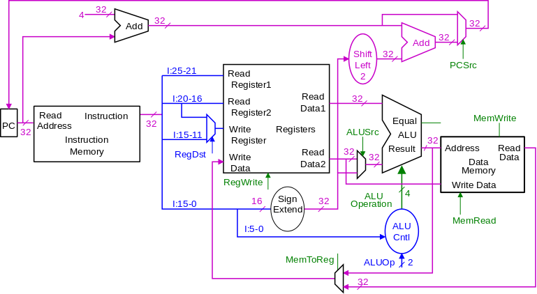
We write I:n-m to represent instruction bits n through m
(inclusive).
For example I:15-0 represents the low order 16 bits of the
instruction, which we recall is the immediate field in an I-type
instruction.
Bits I:31-26, the opcode, have not been used up to this point.
We shall see that the opcode, will play a prominent role when we
determine the control lines.
The Control for the Datapath
Now that we have added the one missing mux and shown how the
instruction bits are divided, two related tasks remain.
  AND     0 0 00
  OR      0 0 01
  Add     0 0 10
  Sub     0 1 10
  Set-LT  0 1 11
  NOR     1 1 00
- We need to generate the control lines used to set the
muxes.
- We need to generate the four ALU control lines: 1-bit Anegate,
1-bit Bnegate and 2-bit OP.
The appropriate values for each of our ALU instructions is shown
in the table on the right.
Don't forget that we use the ALU for instructions such as lw/sw as
well.
Homework: What happens
if we use 0 1 00 for the four ALU control lines?
What if we use 0 1 01?
Question: What information can we use to decide on
the muxes and alu control lines?
Answer: The instruction!
- Opcode field (6 bits).
- For R-type instructions, the funct field (6 bits).
- A total of 12 bits of information.
What must we calculate?
- The 3 ALU control lines (there really are four but we will not
be supporting NOR initially, so we do not
need ANegate).
- One control line for each of the 4 (2-way) muxes shown.
- Two control lines for MemWrite,
and RegWrite.
- A total of 9 (or 10, if we really want NOR)
No problem, just do a truth table.
- 12 inputs so 4096 rows.
- 9 outputs so 21 columns.
- 84K entries.
- HELP!
We again need some inspiration.
A Two-Stage Approach
  ALUOp   Action needed by ALU

  00      Addition (for load word and store word)
  01      Subtraction (for beq)
  10      Determined by funct field (R-type instruction)
  11      Not used
We will let the main control (to be done later) summarize
the opcode for us.
From this summary and the 6-bit funct field, we shall determine the
control lines for the ALU.
Specifically, the main control will summarize the opcode as the
2-bit field ALUOp, whose meaning is shown on the right
Controlling the ALU Given the Summary
How many entries do we have now in the truth table?
- Instead of a 6-bit opcode we have a 2-bit summary.
- We still have a 6-bit function (funct) field (needed for R-type).
- So now we have 8 inputs (2+6) and 3 (or 4, if we want NOR)
outputs.
- 256 rows, 11 columns; 2816 entries.
- Certainly possible for automation ... but we will be clever.
Specifically, we will make great use of don't care
bits.
Some Initial Simplifications
The table on the right shows the work still
required.
| opcode | ALUOp | operation |
funct | ALU action | ALU cntl |
| LW | 00 | load word |
xxxxxx | add | 0010 |
| SW | 00 | store word |
xxxxxx | add | 0010 |
| BEQ | 01 | branch equal |
xxxxxx | subtract | 0110 |
| R-type | 10 | ADD |
100000 | add | 0010 |
| R-type | 10 | SUB |
100010 | subtract | 0110 |
| R-type | 10 | AND |
100100 | and | 0000 |
| R-type | 10 | OR |
100101 | or | 0001 |
| R-type | 10 | SLT |
101010 | set on less than | 0111 |
- We will not be doing NOR so
- We have only 8 MIPS instructions that use the ALU.
- The left bit of ALU cntl (Anegate) is always 0.
Hence, it is not shown in future tables.
- The first two rows of the table above are the same.
Each says that when ALUOp=00, ALU cntl is 0010.
Hence we need only one line.
- When funct is used, its two HOBs are always 10 so are don't care
inputs.
- ALUOp=11 impossible and hence
- 01 = x1
- 10 = 1x
  ALUOp | Funct        ||  Bnegate:OP
  1 0   | 5 4 3 2 1 0  ||  B OP
  ------+--------------++------------
  0 0   | x x x x x x  ||  0 10
  x 1   | x x x x x x  ||  1 10
  1 x   | x x 0 0 0 0  ||  0 10
  1 x   | x x 0 0 1 0  ||  1 10
  1 x   | x x 0 1 0 0  ||  0 00
  1 x   | x x 0 1 0 1  ||  0 01
  1 x   | x x 1 0 1 0  ||  1 11
Applying these simplifications yields the truth table on the right
How should we implement this?
We will do it PLA style (disjunctive normal form, 2-levels of logic)
for each of the three output bits separately.
Specifically, for each output, we will
- First find the minterms, i.e., the cases in which that output
bit is asserted.
- Then produce a circuit for each mini term (an AND of
literals).
- Finally, construct an OR of these ANDs.
Only the first part requires any real work.
  ALUOp | Funct
  1 0   | 5 4 3 2 1 0
  ------+------------
  x 1   | x x x x x x
  1 x   | x x 0 0 1 0
  1 x   | x x 1 0 1 0

  ALUOp | Funct
  1 0   | 5 4 3 2 1 0
  ------+-------------
  x 1   | x x x x x x
  1 x   | x x x x 1 x
BNegate
We start with Bnegate (called Op2 in book).
Question: When is BNegate asserted?
Answer: Those rows in the table above where its bit
(the leftmost output bit) is 1.
That is, rows 2, 4, and 7.
We show those three rows on the right.
Looking again at the full (7-row) table, we notice that, in the 5
rows with ALUOp=1x, F1=1 is enough to distinugish the two rows
where Bnegate is asserted.
This gives the last table for BNegate, again shown on the right.
It has just two rows.
Hence Bnegate is simply ALUOp0 + (ALUOp1 · F1).
  ALUOp | Funct
  1 0   | 5 4 3 2 1 0
  ------+------------
  1 x   | x x 0 1 0 1
  1 x   | x x 1 0 1 0

  ALUOp | Funct
  1 0   | 5 4 3 2 1 0
  ------+------------
  1 x   | x x x x x 1
  1 x   | x x 1 x x x
Op0
Now we apply the same technique to determine when
OP0 is asserted and begin by listing on the right the rows in the
full table where its bit (the rightmost output bit) is set.
As with BNegate, we look back at the full table and study all the
rows where ALUOp=1x, and, within that group of rows, those rows
where OP0 is asserted (the last two rows).
We see that the rows where OP0 is asserted are characterized by
just two Function bits (3 and 0), which reduces the table to that on
the right.
Hence OP0 is (ALUOp1 · F0) + (ALUOp1 · F3)
= ALUOp1 · (F0 + F3)
  ALUOp | Funct
  1 0   | 5 4 3 2 1 0
  ------+------------
  0 0   | x x x x x x
  x 1   | x x x x x x
  1 x   | x x 0 0 0 0
  1 x   | x x 0 0 1 0
  1 x   | x x 1 0 1 0


  ALUOp | Funct
  1 0   | 5 4 3 2 1 0
  ------+------------
  0 0   | x x x x x x
  x 1   | x x x x x x
  1 x   | x x x 0 x x


  ALUOp | Funct
  1 0   | 5 4 3 2 1 0
  ------+------------
  0 x   | x x x x x x
  1 x   | x x x 0 x x


  ALUOp | Funct
  1 0   | 5 4 3 2 1 0
  ------+------------
  0 x   | x x x x x x
  x x   | x x x 0 x x
Op1
Finally, we determine when OP1 is asserted using the
same technique.
However, we shall see that this bit requires more inspiration
than the first two.
Once again the procedure begins by listing on the right those rows
where the relevant bit (the middle output bit) is one.
Right away we get a hint that we have more work to do as five rows
pop up.
As before we study the 5 rows in the original 7-row table that have
ALUOp=1x, and, within that group, those rows where OP1 is asserted
(rows 3, 4, and 7).
We again find that one Funct bit distinguishes when OP1 is asserted,
namely Funct bit 2 (in this case OP1 is asserted when Funct bit 2 is
false).
As a result the 5-row truth table for OP1 reduces to the 3-row
version shown on the right.
Although this truth table would yield a fairly small circuit, we
shall simplify it further.
Recall from the original table, that the x 1 in the second row is
really 0 1.
Although x 1 gives us more freedom than 0 1 in implementing this row
by itself, we are able to simply further by undoing the don't care
and noting that, with 0 1 in the second row, rows 1 and 2 can be
combined to give the table on the right.
Last, we can use the first row to enlarge the scope (and hence
simplify the implementation) of the last row resulting in the final
table on the right.
So OP1 = (ALUOp1)' + (Funct2)'
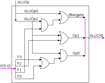
The Circuit
After all the simplification the circuit itself is
very easy and is shown on the right.
Indeed, the simplifications were so successful that we are lead to
question whether this was due to
- Good luck.
- Copious inspiration.
- Well chosen Funct field values by the MIPS engineers.
- A wise selection of instructions to implement by Patterson and
Hennessy.
- Some of each.
Summary and Evaluation
We were given:
- A (well chosen) list of 8 instructions that needed to use the
ALU.
- A 2-bit summary of the opcode that distinguished three cases:
- Load word and Store word.
- Branch on Equal.
- Opcode 0 (the R-types we are implementing)
We will do this 6-bit opcode to 2-bit summary soon.
We calculated the control bits for our ALU.
The resulting circuit was trivial!
But the smarts to make it trivial was non-trivial.
Inspiration again reduced perspiration.
Start Lecture #15
The Main Control
At long last we get to use the opcode (instruction
bits 31-26).
Shown in blue in the diagram below is the main control
, the
logic block that calculates the green control lines that have
appeared above but were floating, i.e., they started from
nothing.
Specifically our task, illustrated in the diagram below, is to
calculate the following eight bits.
(Note that a smaller picture—without the control—was
shown here).
- The select lines for the four muxes (Branch, MemToReg, ALUSrc,
RegDst).
- The write line for the registers (RegWrite).
- The write line for the memory (MemWrite).
- The two ALUOp bits.
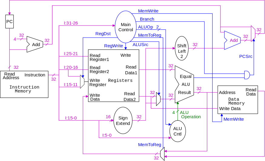
All 8 bits are determined by the opcode.
We show the logic diagram after we illustrate the operation of the
control logic.
Note that the MIPS instruction set is fairly regular.
Most of the fields we need are always in the same place in the
instruction (independent of the instruction type).
- The opcode (called Op[5-0] in the book) is always in bits
31-26.
- The registers to be read are always rs and rt, bits 25-21 and
20-16 (R-type, beq, sw).
- The base register used for calculating the effective address
is always rs, bits 25-21 (lw, sw).
- The offset used for calculating the effective address is the
immediate field, which is always imm, bits 15-0.
- Oops: The register to be written is sometimes rt, bits 20-16,
(load) and other times rd, bits 15-11, (R-type).
Hence a mux is needed.
| MemWrite: |
Memory stores the specified value at the specified addr |
| ALUSrc: |
Second ALU operand comes from (reg-file / sign-ext-immediate) |
| RegDst: |
Number of reg to write comes from the (rt / rd) field |
| RegWrite: |
Reg-file stores the specified value in the specified register |
| PCSrc: |
New PC is Old PC+4 / Branch target |
| MemtoReg: |
Value written in reg-file comes from (alu / mem) |
We have just seen how ALUOp is used to calculate the control bits
for the ALU.
The purpose of the the remaining 6 bits
(recall that ALUOp is 2 bits) are described in the table to the
right and their uses in controlling the datapath is shown in the
picture above.
We are interested in four opcodes.
Do a stage play
- Need
volunteers
- One for each of 4 muxes.
- One for PC reg.
- One for the register file.
- One for the instruction memory.
- One for the data memory.
- I will play the control.
- Let the PC initially be zero.
- Let each register initially contain its number (e.g. R2=2).
- Let each data memory word initially contain 100 times its address.
- Let the instruction memory contain (starting at zero).
      add r9,r5,r1 r9=r5+r1   0   5   1   9   0  32
      sub r9,r9,r6            0   9   6   9   0  34
      beq r9,r0,-8            4   9   0   <  -2   >
      slt r1,r9,r0            0   9   0   1   0  42
      lw  r1,102(r2)         35   2   1   <  100  >
      sw  r9,102(r2)         43   2   9   <  100  >
- Go!
The following figures illustrate the play.
Bigger versions of the pictures are
here.
R-type Instructions
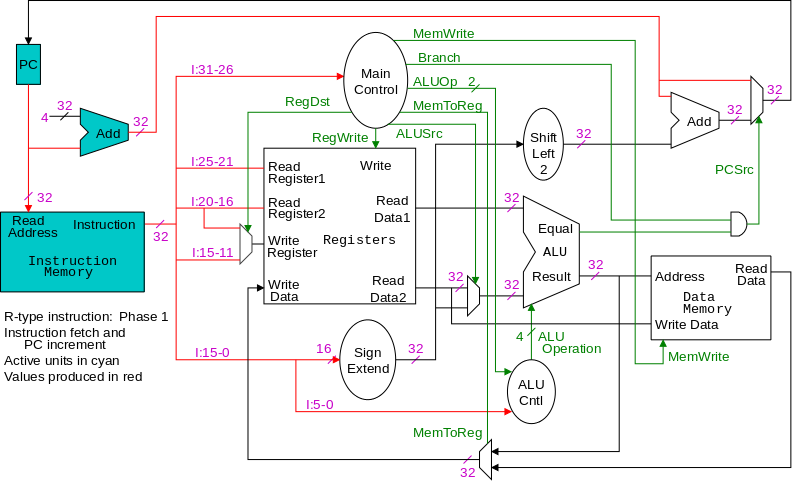
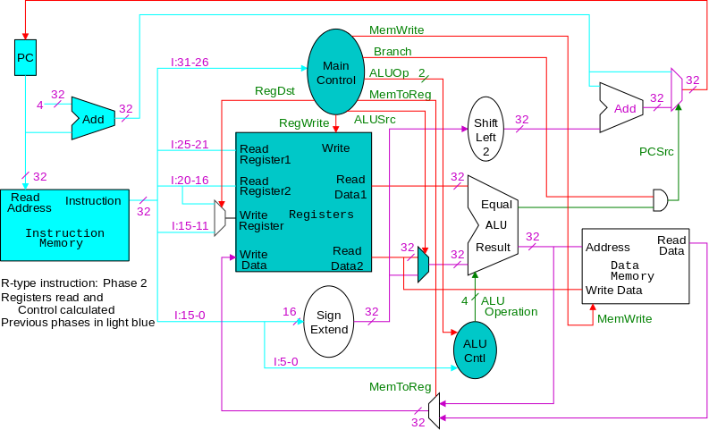
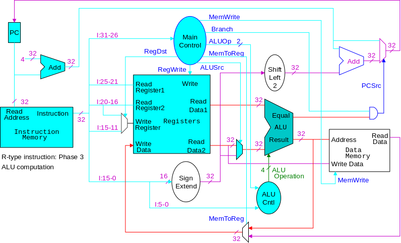
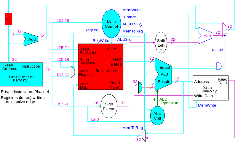
lw Instruction
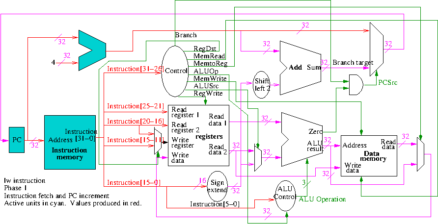
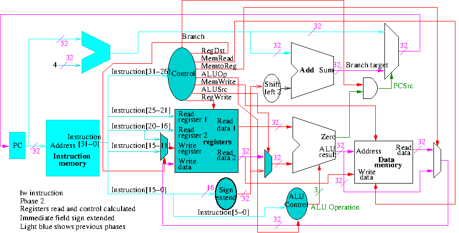
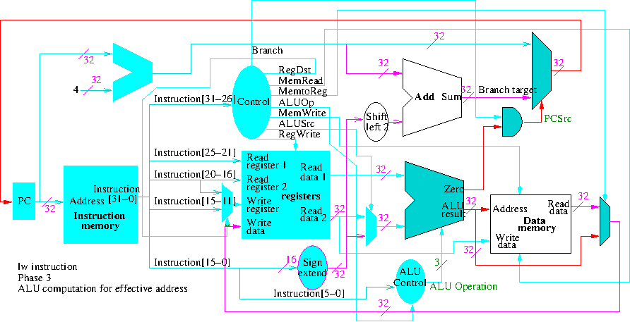
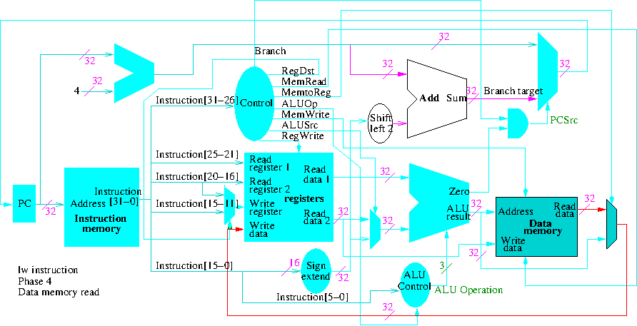
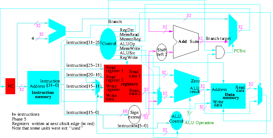
Truth Tables
The following truth table shows, for each of the four opcodes we
are studying, the values needed for each control line.
Recall that we have more than four instructions since we are
implementing several R-type instructions all of which have the same
opcode (opcode zero).
As we have seen, these R-type instructions are distinguished by the
6 Funct bits.
| Instruction |
Op5 | Op4 | Op3 | Op2 | Op1 | Op0 |
RegDst | ALUSrc | MemtoReg | RegWrite |
MemWrite | Branch | ALUOp1 |
ALUOp0 |
|
|
| R-type |
0 | 0 | 0 | 0 | 0 | 0 |
1 | 0 | 0 | 1 | 0 | 0 |
1 | 0 |
| lw |
1 | 0 | 0 | 0 | 1 | 1 |
0 | 1 | 1 | 1 | 0 | 0 |
0 | 0 |
| sw |
1 | 0 | 1 | 0 | 1 | 1 |
X | 1 | X | 0 | 1 | 0 |
0 | 0 |
| beq |
0 | 0 | 0 | 1 | 0 | 0 |
X | 0 | X | 0 | 0 | 1 |
0 | 1 |
| Control | Signal |
R-type | lw | sw | beq |
| Inputs |
Op5 | 0 | 1 | 1 | 0 |
| Op4 | 0 | 0 | 0 | 0 |
| Op3 | 0 | 0 | 1 | 0 |
| Op2 | 0 | 0 | 0 | 1 |
| Op1 | 0 | 1 | 1 | 0 |
| Op0 | 0 | 1 | 1 | 0 |
| Outputs |
RegDst | 1 | 0 | X | X |
| ALUSrc | 0 | 1 | 1 | 0 |
| MemtoReg | 0 | 1 | X | X |
| RegWrite | 1 | 1 | 0 | 0 |
| MemWrite | 0 | 0 | 1 | 0 |
| Branch | 0 | 0 | 0 | 1 |
| ALUOp1 | 1 | 0 | 0 | 0 |
| ALUOp0 | 0 | 0 | 0 | 1 |
The numerous columns, many with wide labels clearly leads to an
extremely wide, and hence awkward table.
To make the table easier to read, Patterson and Hennessy draw this
particular table in a non-standard manner as shown on the right.
The key change is that what was previously the column headings is
now the row headings.
Just for fun, I tried to keep the original format and arrived at
the version shown below.
Don't tell H&P, but I like mine better.
| Instru |
Op5 | Op4 | Op3 |
Op2 | Op1 | Op0 |
Reg | ALU |
Memg | Reg |
Mem |
Branch | ALU |
ALU |
| ction | | | | | | |
Des | Src | toReg | Write | Write |
| Opt1 | Opt0 |
|
|
| R-type |
0 | 0 | 0 | 0 | 0 | 0 |
1 | 0 | 0 | 1 | 0 |
0 | 1 | 0 |
| lw |
1 | 0 | 0 | 0 | 1 | 1 |
0 | 1 | 1 | 1 | 0 |
0 | 0 | 0 |
| sw |
1 | 0 | 1 | 0 | 1 | 1 |
X | 1 | X | 0 | 1 |
0 | 0 | 0 |
| beq |
0 | 0 | 0 | 1 | 0 | 0 |
X | 0 | X | 0 | 0 |
1 | 0 | 1 |
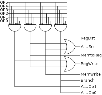
The Circuit
As always, given a truth table, it is quite easy to
produce logic equations and a logic diagram, both in PLA style
(i.e., using 2-levels of logic.
The circuit, drawn in PLA style is shown on the right.
Homework: In a previous
homework, you modified the datapath to support addi and a variant of
lw.
Determine the control needed for these instructions.
The Logic Equations
This is easy given the circuit.
  RegDst   = Op5'Op4'Op3'Op2'Op1'Op0'
  ALUSrc   = Op5 Op4'Op3'Op2'Op1 Op0  + Op5 Op4'Op3 Op2'Op1 Op0
  MemtoReg = Op5 Op4'Op3'Op2'Op1 Op0
  RegWrite = Op5'Op4'Op3'Op2'Op1'Op0' + Op5 Op4'Op3'Op2'Op1 Op0
  MemWrite = Op5 Op4'Op3 Op2'Op1 Op0
  Branch   = Op5'Op4'Op3'Op2 Op1'Op0'
  ALUOp1   = Op5'Op4'Op3'Op2'Op1'Op0'
  ALUOp0   = Op5'Op4'Op3'Op2 Op1'Op0'
Implementing a J-type Instruction, Unconditional Jump
Recall the jump instruction.
  opcode  addr
  31-26   25-0
Addr is a word address.
Since the machine is byte addressable, we need to shift the address
left 2 bits (filling the right with zeros).
The address in the instruction is 26 bits.
When shifted and and 0 filled, the result is 28 bits.
But the machine has 32-bit addresses.
Where do the remaining 4 bits come from?
Answer: The high order 4 bits of the new address are set equal to
the high order 4 bits of the previous instruction
(after incrementing the latter by 4).
This is quite easy to implement as seen in the following diagram.
Basically all that is added to the datapath is one mux and its
associated control line (plus a few wires).
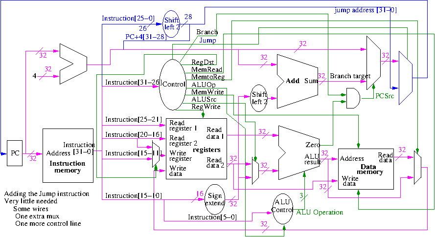
Start Lecture #16
Midterm Exam
Start Lecture #17
What's Wrong, i.e., Why Isn't This Used?
Some instructions are likely slower than others and we must set the
clock cycle time long enough for the slowest.
The disparity between the cycle times needed for different
instructions is quite significant when one considers implementing
more difficult instructions, like divide and floating point ops.
Actually, if we considered cache misses, which result in references
to external DRAM, the cycle time ratios would exceed 100.
Possible solutions
- Variable length cycle.
How would this be implemented?
- Asynchronous logic
Self-timed
logic.- No clock.
Instead each signal (or group of signals) is coupled with
another signal that changes only when the first signal (or
group) is stable.
- Hard to debug.
- Multi-cycle instructions.
- More complicated instructions have more cycles.
- Since only one instruction is executed at a time, can
reuse a single ALU and other resourses during different cycles.
- Earlier editions of the book covered this right at this
point.
Removed in the 4e.
Instead multicycle caches are covered.
- Pipeline the cycles.
- Recall the
stage plays
we did earlier.
You can see that the instructions execute in phases: That
is, first the instruction is fetched, then the registers are
read, then the ALU is accessed, etc.
- The idea behind pipelining, is that when the first
instruction accesses the registers, we have a second
instruction being fetched.
Then, when the first instruction is accessing the ALU, the
second is reading the registers, and a third instruction is
fetched.
- So we make each part of the instruction execution
(instruction-fetch, register-read, alu-execute, ...) a
separate cycle.
- Since at one time we will have several instructions
active, each at a different cycle, the resources can't
be reused (e.g., more than one instruction might need to
do a register read/write at one
time).
- Pipelining is more complicated than the single cycle
implementation we did.
- It was the basic RISC technology on the 1980s.
- A pipelined implementation of the MIPS CPU is our next task,
but, after a short introduction to pipelining, we take a
detour to understand performance and performance measurement a
little better.
- Multiple datapaths (superscalar).
- Issue several instructions each cycle and the hardware
figures out dependencies and only executes instructions when the
dependencies are satisfied.
- Much more logic required, but conceptually not too
difficult providing the system executes
instructions in order.
- Pretty hairy if out of order (OOO) execution
is permitted.
- Current high end processors are all OOO superscalar
(and are indeed pretty hairy).
- A very modern consideration is that performance per
transistor is going down and that it
would/might be better to have many simple processors on
a chip rather that one or a few complicated ones
- Moreover, the complicated processors consume a great deal
of power, an increasing problem.
- VLIW (Very Long Instruction Word).
- User (i.e., the compiler) packs several instructions
into one
superinstruction
called a very long
instruction.
- User guarentees that there are no dependencies within
a superinstruction.
- Hardware still needs multiple datapaths (indeed the
datapaths are not so different from superscalar).
- The hairy control for superscalar (especially OOO
superscalar) is not needed since the dependency checking
is done by the compiler, not the hardware.
- Was proposed and tried in 80s, but was dominated by
superscalar.
- A comeback (?) with Intel's EPIC (Explicitly Parallel
Instruction Computer) architecture.
- Called IA-64 (Intel Architecture 64-bits); the
first implementation was called Merced and now has a
funny name (Itanium).
It became available in the 1990s.
- It has other features as well (e.g. predication).
- The x86, Pentium, etc are called IA-32.
- Has not done well and appears dead/dieing.
4.5 An Overview of Pipelining
Patterson and Hennessy give a real-world example of pipeline based
on doing multiple loads of laundry.
For variety, I will present a different example, based on
sandbagging a river to prevent (or at least minimize) flooding.
The Sandbagging Problem
We have a huge quantity of dirt in the western part of an old gray
town and a river with rising water in the eastern part.
Since we anticipated the possibility of the river rising, we
stockpiled empty burlap bags near the dirt and we have a small loop
of train tracks running between the dirt and the river.
We purchased a bright red cart and placed it on the track near
the dirt.
A Single Cycle Solution
If we adopted the method of our single cycle MIPS
implementation we would proceed as follows.
- We fill a bag with dirt and put it on the cart.
- We send the cart east.
- When the cart arrives at the eastern part of the loop, we carry
the bag of dirt to the river.
- We place the bag of dirt at the correct position.
- We send the empty cart west.
- Repeat.
If we make the simplifying assumption that each of the five steps
takes the same time, say T minutes, then it takes
5T minutes to complete job for one bag of sand.
A Pipelined Solution
We can do better than the approach just given; we
can pipeline the activities.
To do this we need five carts not just one, and more people.
Initially all five carts are near the dirt pile.
We start the same by filling the first bag of dirt and placing it
on the first cart.
When we start the cart carrying bag 1 east (step 2 of bag 1
begins) we can immediately start to fill bag 2 (step 1 of bag 2
begins).
When start to carry bag 1 to the river (step 3 of bag 1 begins), we
can start the cart carrying bag 2 east (step 2 of bag 2 begins) and
can start filling bag 3 (step 1 of bag 3 begins).
It gets better.
When starting to place bag 1 at the correct position (step 4 of bag
1 begins), we can
- Start carrying bag 2 to the river (step 3 of bag 2 begins).
- Start sending the cart with bag 3 east (step 2 of bag 3
begins).
- Start filling bag 4 (step 1 of bag 4 begins)
Finally, when sending an empty cart west for the first time (step
5 of bag 1 begins), we can
- Start placing bag 2 at the correct position (step 4 of bag 2
begins).
- Start carrying bag 3 to the correct position (step 3 of bag 3
begins.
- Start sending the cart with bag 4 east (step 2 of bag 4
begins)
- Start filling bag 5 (step 1 of bag 5 begins).
This can continue indefinitely.
Comparison
The second solution seems much better: Instead of a
sand bag being placed onces every 5T minutes, we now place
one every T minutes, a fivefold improvement.
But the time for each sand bag is unchanged; it
remains 5T.
The improvement comes from the fact that we are working on several
sand bags simultaneously.
This is the gain in pipelining.
The overall latency of each operation remains constant (actually it
increases—i.e., gets worse—slightly), but the throughput
increases—i.e. gets better—considerably.
Put another way we can say that pipeline improves performance by
increasing throughput not by
decreasing the time for one instruction.
Pipelining the MIPS Processor
The same idea used for sand bagging and laundry can be applied for
executing computer instructions.
For executing MIPS instructions the pipeline has 5 steps or
stages.
- Fetch the instruction from memory.
- Read the registers and decode the instruction.
- Use the ALU to execute the instruction or compute an
address.
- Access data memory.
- Write a register (with the result).
An Illustrative example
Figure 4.26: Patterson and Hennessy 4e
Approximate times for each pipeline stage.
Instruc-
tion | Instruc-
tion fetch |
Register
read | ALU
Operation |
Data
access | Register
write | Total
time |
| lw | 200 ps | 100 ps | 200 ps |
200 ps | 100 ps | 800 ps |
| sw | 200 ps | 100 ps | 200 ps |
200 ps | | 700 ps |
| R-type | 200 ps | 100 ps | 200 ps |
| 100 ps | 600 ps |
| beq | 200 ps | 100 ps | 200 ps |
| | 500 ps |
The table on the right gives approximate times for each part of
executing the MIPS instructions we have implemented.
Using our single cycle implementation would need make the clock
cycle time 800ps, the time for the longest instruction.
Using a five-stage pipeline, we would need to make the cycle time
200ps, the time of the slowest stage.
Since all instructions go through all 5 stages (even if nothing is
done for that instruction during one or more stages), every
instruction will take 1000ps=1ns from beginning to end.
This sounds worse!
Indeed, it is worse if you judge performance by the time for one
instruction.
But, as we mentioned before, the more relevant measure is the
throughput, i.e., the number of instructions executed in one
second.
Let's look at executing a three instruction program that adds value
in register 3 to a location in memory.
  lw  $r1, 50($r2)   // uses all 5 stages
  add $r1, $r1, $r3  // no data access
  sw  $r1, 50($r2)   // no register write
Our single stage implementation requires 3 * 800ps = 2400ps to
execute these three instructions.
The instruction execution time is 800ps and the throughput is
3 instructions / (2400 * 10-12 second) = 1.25 * 109 instructions/second
The pipelined execution requires 1400ps; the instruction execution
time is 1000ps; and the throughput is
3 instructions / (1400 * 10-12 second) ∼ 2.14 * 109 instructions/second
The result would get better if we used a bigger example.
Indeed the asymptotic speedup is 4 since the single cycle
implementation starts one instruction every 800ps and the pipelined
implementation starts one instruction every 200ps.
Remember that real programs execute (at least) billions of
instructions so the value obtained for such programs would be
extremely close to 4.
Designing Instruction Sets for Pipelining
The MIPS instruction set was designed to ease pipelining in the
following ways.
- All instructions are the same length.
This facilitates fetching instruction 2 before have really begun
executing instruction 1.
If you needed to decode the instruction to determine its length,
I-fetch could not begin for an instruction until the previous
instruction was decoded.
- Very few formats and source register fields are always in the
same place.
If the source fields depended on the opcode, we could not read the
registers right after I-fetch, but would need another pipeline
stage to determine which registers to read.
Note that it is not a problem that we might
actually read a register whose value is not needed.
- Memory operands appear only in loads and stores.
If, for example, you could add a register to a memory location, we
would need to use the ALU twice (once to calculate the memory
address; a second time to do the actual addition).
This would need another pipeline stage (and a second ALU).
- Operands are word aligned in memory.
When we learn about memory, we will see that this permits a
single 32-bit data-access.
Pipeline Hazards
The example shown above gives a unrealistic view of pipeline since
we have not discussed hazards that can delay an instruction
because it cannot execute the next pipeline stage right away.
Structural Hazards
This occurs when the hardware cannot execute all the actions
required during one cycle.
MIPS was designed to minimize this possibility, but consider a
different design that had one memory instead of the two as in MIPS.
Then, if the first instruction was lw, it would be
accessing this memory during cycle 4 to read the data.
But at the same time, the 4th instruction needs to do an I-fetch.
The resulting contention for the combined data-instruction memory is
a structural hazard.
Data Hazards
Consider the familiar statement A = B+C; found in most
languages.
It would most likely be translated by the compiler into an
instruction sequence like the one shown on the right.
Assume the sequence starts at cycle 1.
Then during cycle 4, the add instruction reads registers
$r1 and $r2.
But those registers are not written with the required values until
cycles 5 and 6.
Hence the third instruction encounters a data hazard at its 2nd
cycle, which causes the pipeline to stall for three cycles until
cycle 7 when the add can perform its second step.
Such stalls are often called bubbles
in the pipeline.
Start Lecture #18
Forwarding (Bypassing)
  add $r1,$r1,$r2
  add $r1,$r1,$r3
Consider the two instruction sequence on the right
that replaces register r1 with the sum of the first three registers.
The second instruction adds the third register to what should be the
sum of the first two.
Looking at a cycle-by-cycle picture of the pipeline (draw this on
the board) we see that the second instruction reads register r1
during cycle 3 (its second cycle).
But that sum will not appear in register r1 until the fifth
cycle.
However, if we look again at the cycle-by-cycle picture,
we see that the sum is calculated during cycle 3
(the 3 stage of the first instruction) and not actually
used until cycle 4 (the third stage of the 2nd
instruction).
As a result one could run a wire from the end of stage 3 to the
beginning of stage 3 (and add a mux and some serious control logic)
and get the value there in time.
We say the value has been forwarded from the first
instruction to the second or that it has bypassed some of
the steps.
In this case the solution was perfect, no bubble remains.
Homework: How would
forwarding be used in the previous 4-instruction sequence?
Do any bubbles remain?
Control Hazards
   beq $r1,$r2,L
   some instructions
L: some other instructions
Consider the conditional branch shown on the right.
During cycle 2 we need to fetch the 2nd instruction to execute, but
we don't know what that instruction is since we don't know yet if
the branch will be taken.
We won't know until the end of cycle 3, when the ALU has determined
if registers r1 and r2 are equal.
We could guess that the branch will not be taken and start
executing some instructions
.
If we guess wrong, we must throw out the work we did based on the
guess.
This hazard has lead to a large field of study called
branch prediction
that uses sophisticated techniques to make
a more intelligent (i.e., a more-likely-to-be-correct) guess as to
whether or not the branch will be taken.
Pipeline Overview Summary
Pipelining is an important component in the processor designer's
toolbox; all modern microprocessors use it.
Pipelining permits the execution of consecutive instructions to be
overlapped.
Although no instruction is itself sped up (indeed some are slowed
down), the throughput is increased significantly.
Hazards can greatly decrease the potential improvement of
pipelining; a well designed ISA can make hazards easier to deal
with, but in any case hazards complicate the design of modern
high-performance processors.
Homework: 4.6.1, 4.6.2,
4.7.1, 4.7.2, 4.9.1-3.
4.6 Pipelined Datapath and Control
Remark: We only sketch some ideas in the rest of
this chapter.
For a complete treatment, read the book carefully.
The diagram below shows the datapath divided into the
same 5 pipeline stages we just studied
.
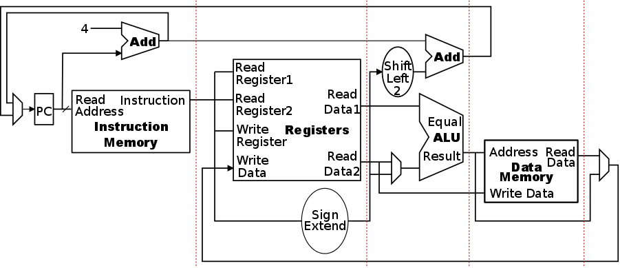
These stages are normally referred to as:
- IF: Instruction fetch.
- ID" Instruction decode / register read.
For MIPS the former is quite easy; for other ISAs, less so.
- EX: Execute / Address Calculation.
- MEM: Memory Access.
- WB: Write Back.
Write the result back into the register file.
The next step is to capture the state after each stage.
This means that we need to replace the simple dotted red lines,
which were just for our visualization by pipeline registers that
hold all the values produced by each stage
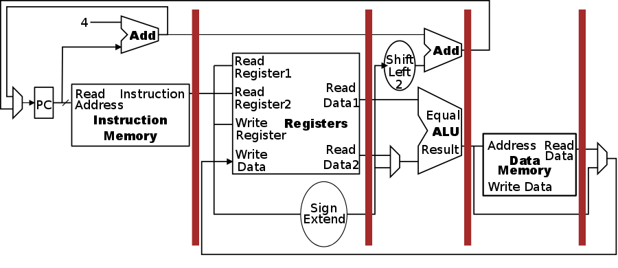
Now you can do another stage play and see that, at the beginning of
each stage, the pipeline registers are read and, at the end of each
stage, they are written.
There are various subtleties that must be addressed.
For example, the register file is written during the fifth pipeline
stage, but the register number is read from the
instruction during the first stage.
Hence, by the time the fifth stage is executed, the register number
is from a later instruction.
This particular problem is fixed by moving the write register
number from pipeline register to pipeline register as the
instruction moves through the pipeline.
At the fifth stage, the register number is sent from
the last pipeline register to the write register input of the
register file.
You might wonder why there are only 4 pipeline registers since
there are five stages.
The answer is that all the fifth stage does is write a register so
this value is being saved for subsequent instructions and no
pipeline register is needed at the end of stage 5.
Graphically Representing Pipelines
The last diagram above represents what is called a
single-clock-cycle pipeline diagram.
Diagrams such as the one on the right (which we have already
discussed) are called multiple-clock-cycle pipeline diagrams
.
The later are easier to follow, but supply fewer details.
Pipelined Control
We already calculated the control lines.
The trouble is that we calculate them at the beginning, but use them
in subsequent stages.
Hence they must be passed from pipeline register to pipeline
register as the instruction moves along the pipeline.
4.7 Data Hazards: Forwarding versus Stalling
Data Hazards and Stalls
4.8 Control Hazards
Assume Branch Not Taken
Reducing the Delay of Branches
Dynamic Branch Prediction
Pipeline Summary
4.9 Exceptions
How Exceptions are Handled in the MIPS Architecture
Exceptions in a Pipelined Implementation
4.10 Parallelism and Advanced Instruction-Level Parallelism
The Concept of Speculation
Static Multiple Issue
An Example: Static Multiple Issue with the MIPS ISA
Dynamic Multiple-Issue Processors
Dynamic Pipeline Scheduling
Power Efficiency and Advanced Pipelining
4.11 Real Stuff: the AMD Opteron X4 (Barcelona) Pipeline
4.12 Advanced Topic: an Introduction to Digital Design Using a
Hardware Design Language to Describe and Model a Pipeline and More
Pipelining Illustrations
4.13 Fallacies and Pitfalls
Three points are made
- Fallacy: Pipelining is easy.
Pipelining is easy conceptually but the details are
challenging, to say the least, and have caused many bugs.
- Fallacy: Pipelining can be implemented independent of
technology.
Of course it can be implemented independent of technology, but the
best implementation has changed several times since 1980 due to
first more resources (transistors, memory) becoming available, and
more recently due to power limitations.
- Pitfall: Failure to consider instruction set design can
adversely affect pipelining.
For example, varying length instructions make it hard to find the
next instruction.
4.14 Concluding Remarks
We have seen how to design the datapath and control for a subset of
the MIPS processor using a single-cycle strategy.
Although successful this simple implementation is too slow so we
investigated, to a limited extent, a more aggressive, pipelined
implementation.
In addition to pipelining, modern designs are
multiple-issue/superscalar.
That is, they issue several instructions each cycle and hence have
several instructions performing each pipeline stage and thus can
have very many instructions active (in flight
) at one
time.
This, coupled with out-of-order execution, which we haven't
discussed, complicates the design and increases the power usage
considerably.
Design complexity may have already already hit and passed its peak.
Power concerns have causes all the major players to cut back on the
complexity of their designs.
4.15 Historical Perspective and Further Reading
Chapter 1 Computer Abstractions and Technology (Revisited)
1.1 Introduction
Read.
1.2 Eight Great Ideas in Computer Architecture
Done.
1.3 Below Your Program
Read.
1.4 Under the Covers
Read.
1.5 Technologies for Building Processors and Memory
Read, but we don't emphasize technology.
Defining Performance
Throughput measures the number of jobs
per day/second/etc that can be accomplished.
Response time measures how long an individual job
takes.
- A faster machine improves both metrics (increases throughput and
decreases response time).
- Normally anything that improves (i.e., decreases) response
time for each job improves (i.e., increases) throughput.
- But the reverse isn't true.
For example, adding a processor likely to increase throughput
more than it decreases response time.
- We will be concerned primarily with response time.
We define Performance as 1 / Execution
time.
Relative Performance
We say that machine X is n times faster than machine Y or
machine X has n times the performance of machine Y if
the execution time of a given program on X = (1/n) * the
execution time of the same program on Y.
But what program should be used for the comparison?
Various suites have been proposed; some emphasizing CPU
integer performance
, others floating point performance
,
and still others I/O performance
.
Measuring Performance
How should we measure execution time?
- CPU time.
- This includes the time waiting for memory.
- It does not include the time waiting for I/O as this
process is not running and hence using no CPU time.
- Should we include
system time
, i.e., time when the
CPU is executing the operating system
on behalf of the user program or just the
time when the program is executing in user-mode?
- Elapsed time on an otherwise empty system.
- Elapsed time on a
normally loaded
system.
- Elapsed time on a
heavily loaded
system.
We mostly employ user-mode
CPU time, but this
does not mean the other metrics are worse.
Cycle time vs. Clock rate.
- Recall that cycle time is the length of a cycle and hence is a
unit of time.
- For modern (non-embedded) computers it is expressed
in nanoseconds, abbreviated ns,
or picoseconds, abbreviated ps.
- One nanosecond is one billionth of a second = 10-9
seconds.
- One picosecond is one trillionth of a second = 10-12
seconds.
- Other units of time are microsecond, abbreviated us, which
equals 10-6 seconds, and millisecond, abbreviated ms,
which equals 10-3 seconds.
- Embedded CPUs often have their cycle times expressed in
microseconds; the time required for a single I/O (disk access)
is normally expressed in milliseconds.
- Electricity travels about 1 foot in 1ns (in normal media).
- The clock rate tells how many cycles fit into
a given time unit (normally in one second).
- So the natural unit for clock rate is cycles per second.
This used to be standard unit and was abbreviated CPS.
- However, the world has changed and the new name for the same
thing is Hertz, abbreviated Hz.
One Hertz is one cycle per second.
- For modern (non-embedded) CPUs the rate is normally expressed
in gigahertz, abbreviated GHz, which equals one billion
hertz = 109 hertz.
- For older or embedded processors the rate is normally
expressed in megahertz, abbreviated MHz, which equals
one million hertz.
What is the cycle time for a 700MHz computer?
- 700MHz means 700 million cycles per second
- Hence 700 million cycles = 1 second
- 7*108 cycles = 1 second
- 1 cycle = 1/(7*108) seconds = 10/7 *
10-9 seconds ~= 1.4ns
What is the clock rate for a machine with a 10ns cycle time?
- 1 cycle = 10ns = 10-8 seconds.
- 108 cycles = 1 second.
- Rate is 108 cycles/second =
108 Hz = 100 * 106 Hz =
100MHz = 0.1GHz.
Start Lecture #19
The Classic CPU Performance Equation
The execution time for a given job on a given computer is
  (CPU) execution time = (clock cycles required) * (cycle time)
                       = (clock cycles required) / (clock rate)
Since the number of clock cycles required equals the number of
instructions executed times the average number of cycles in each
instruction, we can write this equation in other equivalent
forms.
An extremely common acronym is CPI, standing for cycles per
instruction.
Thus we have.
  CPU Time (in seconds) =  #Instructions * CPI * Cycle_time (in seconds).
  CPU Time (in ns)      =  #Instructions * CPI * Cycle_time (in ns).
  CPU Time (in seconds) =  #Instructions * CPI / Clock_Rate (in Hz).
What is the CPI?
In our single cycle implementation, the number of cycles required
is just the number of instructions executed.
That is, the CPI is 1.
Similarly, if every instruction took 5 cycles, the number of cycles
required would be five times the number of instructions
executed.
But real systems are more complicated than that!
- Some instructions take more cycles than others.
- With pipelining, several instructions are in progress at different
stages of their execution.
- With super scalar (or VLIW) many instructions are issued (begin
execution) at once.
- Since modern superscalars are also pipelined we have many, many
instructions executing at once.
After extensive measurements, one calculates for a given machine
the average CPI (cycles per instruction).
We shall sometimes assume this average CPI actually applies to all
instructions.
Other times we shall say something like
Assume there are two classes of instructions.
Class A instructions require 4 cycles to execute;
class B instructions require 3 cycles to execute.
Assume an execution of program P involves 30% class A instructions
and 70% class B.
What is the (average) CPI for this execution?
The number of instructions required for a given program depends on
the instruction set.
For example, assume we want to add the contents of register 1 to a
location X in memory.
Then MIPS would require three instructions; whereas, x86 needs only
one.
  lw  $r3,X
  add $r3,$r1       add X,$r1
  sw  $r3,X
CPI is a good way to compare two implementations of the same
instruction set (also called the same ISA
instruction set architecture
).
IF the clock cycle is unchanged, then
the performance of a given ISA is inversely proportional to the CPI
(e.g., halving the CPI doubles the performance).
Naturally, complicated instructions often take longer to execute.
They require either more cycles or a longer cycle time.
Older machines with complicated instructions (e.g., the Digital
Equipment Corporation VAX, an important machine in the 1980s) had
CPI>>1.
As we have seen, with pipelining we can have many cycles for
each instruction but still achieve a CPI of nearly 1.
Modern superscalar machines often have a CPI less than one.
As a result sometimes one speaks of the IPC or instructions per
cycle
for such machines.
However, we won't use IPC.
- These machines issue (i.e., initiate) many instructions each
cycle.
- They are pipelined so the instructions don't finish for
several cycles.
- If we consider a 4-issue superscalar and assume that all
instructions require 5 (pipelined) cycles, there are up to
5*4=20 instructions in progress (often called in flight) at one
time.
Do on the board the following example from pages 37.
A compiler designer is developing code sequences for a particular
computer.
The computer has three classes of instructions, A, B, and C, which
have CPIs of 1, 2, and 3 respectively.
Note: This is shorthand for saying
Class A instructions, on average, add one cycle to the execution
time
and similarly for classes B and C.
It is not saying that executing one class A instruction takes one
cycle from beginning to end.
Again we see the difference between the latency of a single
instruction and the throughput (instructions per second).
Perhaps it would be better to say that
the cost of a class A instruction is one cycle
.
The compiler writer has a choice of two possible sequences of
machine language instructions as a translation of a particular
high-level language statement.
The first sequence has 2 class A instructions, 1 class B, and 2
class C.
The second sequence has 4 class A and 1 each class B and C.
Which sequence executes the most instructions?
Which is faster?
What is the CPI for each sequence.
Homework: Carefully go
through and understand the example that I just did in class.
Homework: 1.5, 1.6.
1.7 The Power Wall
Covered very briefly.
1.8 The Sea Change: The Switch from Uniprocessors to Multiprocessors
1.9 Real Stuff: Benchmarking the Intel Core i7
As mentioned previously, some instructions take longer than others.
Moreover, some ISAs perform better on certain instructions and other
ISAs perform better on other instructions.
Different application programs use different mixes of
instructions.
It might be, for example, that computer A does great on programs
that reference memory heavily, but poorly on programs dominated by
floating point operations.
In contrast computer B might excel on floating-point, but be
sluggish on memory references.
As you can imagine, computer manufacturers would prefer that
a customer evaluates the company's products by running programs on
which the products do particularly well.
To standardize the measurements, many vendors agreed on certain
sets of benchmarks on which they would provide performance
evaluations.
Perhaps the best know standard benchmarks are those sanctioned by
SPEC (System Performance Evaluation Cooperative).
SPEC actually contains several benchmark suites.
- An integer suite (formally called SPECint, now CINT2006).
- A floating-point suite CFP2006.
- A combination of the above two SPECCPU2006.
- SPECpower, measuring power consumption of servers.
- Others as well.
1.10 Fallacies and Pitfalls
Amhahl's Law
One fallacy is to assume that by fixing part of
the problem, the entire problem is fixed to a very great extent.
For example, assume a simple system with two classes of
instructions
- Floating point instructions, which have a CPI of 10.
- Everything else, which have a CPI of 2.
A new wiz-bang floating-point unit is proposed that speeds
floating-point instructions by a factor of 5 (new CPI is 2), has no
effect on cycle time, and only doubles the cost of the machine.
Sounds great; a speedup of 5 at a cost of only 2!
But just how great is it?
Say the customer is primarily interested in a single application A.
Measurements show that A executes N instructions, 20% of
which are floating point.
To execute application A, the old system takes
.2N * 10 cycles + .8N * 2 cycles = 2N + 1.6N cycles = 3.6N cycles
The new, improved system would take
.2N * 2 cycles + .8N * 2 cycles = .4N + 1.6N cycles = 2N cycles
Since the cycle time hasn't changed, execution time is proportional
to the number of cycles.
Thus the new system is 3.6N / 2N = 1.8 times faster for
only
twice the price.
No sale!
Speedup Using Multiple Computers (the Original Amdahl's Law)
NOAA has a new computer program that is predicting tomorrow's
weather very well, but the computation takes a week, which makes the
results useless.
They need to reduct the 168 hours (one week) to 1 hour.
They know that the program spends 99% of its time doing material
that can be partitioned evenly on up to a thousand processors.
Since they need a speedup of at least 168 and have the money, they
decide to buy 1000 processors.
How long does the program now take to run?
Answer: 1% of 168 hours is 1.68 hours; 99% of 168 hours is 166.32
hours.
The 1000 processors cooperate on the second piece and reduce it to
166.32/1000=.16632 hours.
However, the small 1% piece isn't be sped up at all and still takes
1.68 hours.
So the entire job takes 1.68+.16632 = 1.84632 hours, which is
exceeds the 1 hour requirement.
The 1000 processors gave a speedup of only 168/1.84632 ∼
91.
Homework: What would the speedup
be if they purchased only
100 processors?
Power
MIPS vs Time
MIPS is an acronym abbreviating Millions of Instructions Per
Second.
It is a unit of rate or speed (like MHz); it is NOT
a unit of time (like ns.).
As its full name suggests, MIPS is defined as
how many million instructions were executed / how many seconds were required
This is the same as
the number of instructions executed / the number of microseconds used
The instructions we have been studying (lw, R-type, etc) are those
of the MIPS computer company.
That usage of the word MIPS is different from the acronym above, but
the company's founders certainly knew about the acronym above.
Indeed, the company started with a Stanford research project
headed by Hennessy.
This project was called MIPS standing for Microprocessor without
Interlocked Pipeline Stages.
However, the microprocessors produced by the MIPS
company did have interlocked pipeline stages.
At roughly the same time, Patterson headed a research project
called RISC standing for Reduced Instruction Set Computer.
Sun Microsystems was to an extent based on this research project.
Problems with the MIPS Rating
MIPS only counts instructions and does not take into account that
some ISAs require more instruction than other ISAs to solve the same
problem.
For example, we saw that adding a register to a memory location
takes 1 instruction on an x86 ISA but three on a MIPS.
If the single instruction took one microsecond, the x86 would
achieve a 1 MIPS rating.
If the three instructions took a total of 2 microseconds, the MIPS
computer would achieve a 1.5 MIPS rating, much better than the x86
even though it required twice as long to accomplish
the same task.
For this reason, the MIPS least should not be used to compare
systems with different ISAs.
Even with a fixed ISA there are difficulties with MIPS.
As with many computer ratings, the program used is important.
A program that has predominately fast instructions will achieve a
higher MIPS rating that a program that has predominately slow
instructions.
A new sophisticated compiler might be able to reduce the number of
instructions needed to complete a program and also reduce the total
execution time.
Clearly a good thing.
But, if the instructions eliminated were the fastest ones, then the
MIPS rating would go down even though performance went up!
To say it in reverse, it is often the case that if one padded a
program with NOPs (which are very fast), the program would have
exactly the same effect, would take longer, would execute more
instructions, but yet would likely achieve a higher
MIPS rating than the original.
MFLOPS (Megaflops)
For numerical calculations floating point operations are often the
ones you are interested in; the others are overhead
(a very
rough approximation to reality).
For this reason the MFLOPS (Millions of FLoating point OPerations
per Second) was introduced.
It has similar problems to MIPS.
- The same program needs different numbers of floating point
operations on different machines (e.g., is sqrt one instruction
or several?).
- Compilers affect the MFLOPS rating.
- MFLOPS is not as bad as MIPS in one respect.
Adding NOPs lowers the MFLOPs rating.
- But you can insert unnecessary floating point ADD instructions
and this will probably raise the MFLOPS rating.
Question: Why is this likely to raise the MFLOPS
rating?
Answer: Because it will lower the percentage
of overhead
(i.e., non-floating point) instructions and
floating-point ADD is probably the fastest floating-point
instruction.
Benchmarks
Benchmarks are better than MIPS or MFLOPS, but still have
difficulties.
- It is hard to find benchmarks that represent your future
usage.
- Compilers can be
tuned
for important benchmarks.
- Benchmarks can be chosen to favor certain architectures.
- If your processor has a 256KB cache (caches are our next
topic) and your competitor's has a 128MB cache, you try to
find a benchmark that frequently accesses a region of memory
having size between 128KB and 256KB (so that it fits into your
cache but not theirs).
- If your processor has a 64MB cache that is 2-way set
associative (defined later) and your competitor's has a 256KB
cache that is direct mapped (i.e., 1-way set associative),
then you choose a benchmark that frequently accesses exactly
two 30KB arrays separated by an exact multiple of 256KB.
(These arrays will fit harmoniously in your cache, but will
collide in theirs).
1.11 Concluding Remarks
Homework: Read this
(very short) section.
1.12 Historical Perspective and Further Reading
Chapter 5: Large and Fast: Exploiting the Memory Hierarchy
Homework: Read Chapter
5.
Note: Perhaps the chapter should be entitled
Large vs. Fast
.
5.1: Introduction
An ideal memory is
- Big (in capacity; not physical size).
- Fast.
- Cheap.
- Impossible.
Unable to achieve the impossible ideal we use a
memory hierarchy consisting of
- Registers.
- Cache (really L1, L2, and L3).
- (Central or Main) Memory.
- Disk.
- Archive (e.g. Tape).
... and try to satisfy most references in the small fast memories
near the top of the hierarchy.
There is a capacity/performance/price gap between each pair of
adjacent levels.
We will ignore price and emphasize the cache-to-memory gap.
- In modern systems there are many levels of caches so we should
study the registers-to-L1 gap, the L1-to-L2 gap, the L2-to-L3 gap,
and the L3-to-memory gap.
- We will largely ignore L3, but will study, the registers-to-L1
gap, the L1-to-L2-gap, and the L2-to-memory gaps
- Similar considerations to those we shall study apply as well
to the other gaps (e.g., memory-to-disk, when demand paging
techniques are applied).
This last is the gap studied in OS classes such as 202/2250.
- But the terminology is often different, e.g., in architecture we
evict cache blocks or lines whereas in OS we evict pages.
- As in past semesters my OS class is studying
the same thing
at roughly the same time as my architecture
class, but with different, almost disjoint, terminology.
We observe empirically (and teach in OS).
- Temporal Locality: The word referenced now is likely to be
referenced again soon.
Hence it is wise to keep the currently
accessed word handy (high in the memory hierarchy) for a while.
- Spatial Locality: Words near the currently referenced
word are likely to be referenced soon.
Hence it is wise to prefetch words near the currently referenced
word and keep them handy (high in the memory hierarchy) for a
while.
Start Lecture #20
A cache is a small fast memory between the
processor and the main memory.
It contains a subset of the contents of the main memory.
A Cache is organized in units of blocks
or lines.
Common block sizes are 16, 32, and 64 bytes.
A block is the smallest unit we can move to/from a cache
(some designs move subblocks, but we
will not discuss such designs).
- We view memory as organized in blocks as well.
The size of a memory block is the same as the size of a cache
block.
If the block size is 16, then bytes 0-15 of memory are in block 0,
bytes 16-31 are in block 1, etc.
- Transfers from memory to cache and back are one block.
- Big blocks make good use of spatial locality.
- If you remember memory management in OS, think of pages and page
frames.
- The terminology in memory management is:
Pages are
located in the big slow disk; frames are in the small fast
(main) memory.
- The terminology in caches is:
Memory blocks are located
in the big slow (main) memory; cache blocks (or cache lines)
are located in the small fast cache.
A hit occurs when a memory reference is found in the upper level
(small, fast) of the memory hierarchy.
Definitions
- We will be interested in cache hits (OS courses
study page hits), when the reference is found in the cache
(OS: when found in main memory).
- A miss is a non-hit (however, in OS we call it a
fault).
- The hit rate is the fraction of memory references
that are hits.
- The miss rate is 1 - hit rate, which is the
fraction of references that are misses.
- The hit time is the time required for a hit.
- The miss time is the time required for a miss.
- The miss penalty is miss time - hit time.
Addressing Bytes, (4-byte) Words, and Blocks
Consider the following address (in binary).
10101010_11110000_00001111_11001010.
This is a 32-bit address.
I used underscores to separated it into four 8-bit pieces just to
make it easy to read; the underscores have no significance.
Machine addresses are non-negative (unsigned) so the address above
is a large positive number (greater than 2 billion).
All the computers we shall discuss are byte addressed.
Thus the 32-bit number references a byte.
So far, so good.
The (4-Byte) Word Addressed and the Byte Offset
We will always assume that each word is four bytes.
That is, we assume the computer has 32-bit words.
This is not always true (many old machines had 16-bit, or smaller,
words; and many new machines have 64-bit words), but to repeat, we
will always assume 32-bit words.
Since 32 bits is 4 bytes, each word contains 4 bytes.
We assume aligned accesses (as does the MIPS architecture we
studied).
This means that a word (a 4-byte quantity) must begin on a byte
address that is a multiple of the word size, i.e., a multiple of 4.
So word 0 includes bytes 0-3; word 1 includes bytes 4-7; word n
includes bytes 4n, 4n+1, 4n+2 and 4n+3; and the four consecutive
bytes 6-9 do NOT form a word.
Question: What word includes the byte address given above,
10101010_11110000_00001111_11001010?
Answer:
10101010_11110000_00001111_110010, i.e, the address divide
by 4.
Question: What are the other bytes in this word?
Answer:
10101010_11110000_00001111_11001000,
10101010_11110000_00001111_11001001,
and
10101010_11110000_00001111_11001011
Question: What is the byte offset of the original
byte in its word?
Answer: 10 (i.e., two), the address mod 4..
Question: What are the byte-offsets of the other
three bytes in that same word?
Answer: 00, 01, and 11 (i.e, zero, one, and
three).
The 32-Byte Block Addressed and the Word and Byte Offset
Blocks vary in size.
We will not make any assumption about the size, other than that it
is a power of two.
For these examples (only), assume each block is 32 bytes.
Since we assume aligned accesses, each 32-byte block has a byte
address that is a multiple of 32.
So block 0 is bytes 0-31, which is words 0-7.
Block n is bytes 32n, 32n+1, ..., 32n+31.
What block includes our byte address
10101010_11110000_00001111_11001010?
Answer:
10101010_11110000_00001111_110, i.e., the byte address
divide by 32 (the number of bytes in the block) or the word address
divided by 8 (the number of words in the block).
5.2 Memory Technology
5.3 The Basics of Caches
We start with a very simple cache organization, one that was used
on the Decstation 3100, a 1980s workstation.
In this design cache lines (and hence memory blocks) are one word
long.
- This does not take advantage of spatial locality so is not
done in modern machines.
- We will soon drop this assumption.
Also in this design each memory block can only go in one specific
cache line.
- This is called a Direct Mapped organization.
- The location of the memory block in the cache (i.e., the
block number in the cache or the
cache block number
) is
the memory block number modulo the number of blocks in the
cache.
- For example, if the cache contains 100 blocks, then memory block
34452 is stored in line 52.
Memory block 352 is also stored in line 52 (but not at the same
time, of course).
- In real systems the number of lines in the cache is a power
of 2 so taking modulo is just extracting low order bits.
- Example: if the cache has 4 lines, the location of a block
in the cache is the memory block number mod 4, which is the
low order 2 bits of the memory block number.
- A direct mapped cache is simple and fast, but has more
misses than the
set associative caches
we will soon
study.
We shall assume that each memory reference issued by the processor
is for a single, complete word.
This assumption holds for the MIPS subset we implemented since the
only memory access were lw and sw.
The full MIPS ISA, however, includes instructions that reference
bytes and halfwords.
Accessing a Cache
On the right is a diagram representing a direct mapped cache with
4 blocks and a memory with 16 blocks.
How can we find a memory block in such a cache?
This is actually two questions in one.
- Is the memory block present in the cache?
- Where in the cache is the memory block, assuming it is
present?
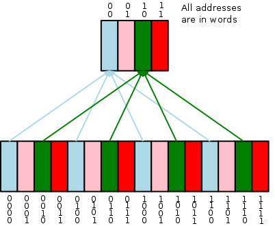
The second question is the easier.
Let C be the number of blocks in the cache.
Then memory block number N can be found only in cache line
number N mod C (it might not be present at
all).
But many memory blocks are assigned to that same cache line.
For example, in the diagram to the right all the
green blocks in memory are assigned to the one green block in the
cache.
So the first question reduces to:
Is memory block N present in cache block N/C?
Referring to the diagram we note that, since only a green memory
block can appear in the green cache block, we know that the last
two digits of the memory block in the green cache block are 10 (the
number of the green cache block).
So to determine if a specific green memory block is in the green
cache block we need the rest
of the memory block number.
Specifically is the memory block in the green cache
block 0010,
0110, 1010,
or 1110?
It is also possible that the green cache block is empty (called
invalid), i.e, it is possible that no memory block is in this cache
block.
- So we need the
rest
of the address (i.e., red digits lost
when we reduced the block number modulo the size of the cache) to
see if the block in the cache is the memory block of interest.
That number is N/C, using the terminology above.
- The cache stores the rest of the address, called the
tag and we check the tag when looking for a block.
- Since we will always choose C to be a power of 2, the
tag (N/C) is simply the high order bits of N.
- Also stored is a valid bit per cache block so that we
can tell if there is a memory block stored in this cache
block.
When the system is powered on, all the cache blocks are invalid so
all the valid bits are off.
On the right is an example from the book (page 386).
It refers to figure 5.8, which is an enlarged version of the example
diagram above.
Figure 5.8 has C=8 (rather than 4) and M=32
(rather than 16).
In both the diagram above and the example from the book, we
have M/C=4 memory blocks eligible to be stored in each
cache block.
Thus there are two tag bits for each cache block.
| Addr(10) | Addr(2) | hit/miss | block# |
|---|
| 22 | 10110 | miss | 110 |
| 26 | 11010 | miss | 010 |
| 22 | 10110 | hit | 110 |
| 26 | 11010 | hit | 010 |
| 16 | 10000 | miss | 000 |
| 3 | 00011 | miss | 011 |
| 16 | 10000 | hit | 000 |
| 18 | 10010 | miss | 010 |
- The example gives a sequence of memory references.
- Do this example on the board showing the addresses stored in the
cache at all times.
The cache is initially empty, i.e., all cache blocks are
invalid.
- Also show the tags.
- In the table on the right, all the addresses are word
addresses.
For example the reference to 3 means the reference to word 3
(which includes bytes 12, 13, 14, and 15).
- Naturally, if a reference is a hit, the current memory block
remains assigned to this cache block (what other memory block
could you choose to assign?).
- If the reference experiences a miss because the cache block is
invalid, we assign this memory block to the cache block (there
are no other contenders).
- If reference experience a miss and the cache block is valid, we
have a dilemma.
Should we leave the existing memory block in the cache block or
should we replace it with the newly referenced cache block.
Our choice (in this example, not in all designs) is to discard the
current contents of the cache block and let the new reference
takes its place.
- Remember that in this very simple design, we have a
direct-mapped cache with block size one word.
Also, all memory references are for one word.
I often abbreviate this situation by saying blksize=refsize=1.
Cache Contents, Hits, and Misses
Shown on the right is a eight entry, direct-mapped cache with block
size one word.
As usual all references are for a single word (blksize=refsize=1).
In order to make the diagram and arithmetic smaller the machine has
only 10-bit addressing (i.e., the memory has only
210=1024 bytes), instead of our usual 32-bit
addressing.
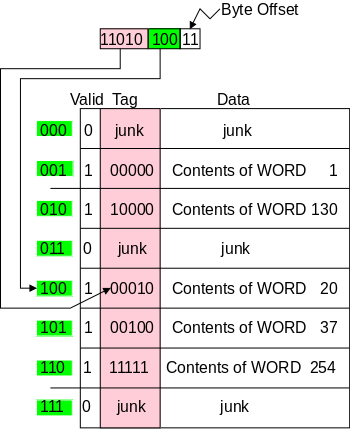
Above the cache we see a 10-bit address issued by the processor.
There are several points to note.
- The valid bit.
If this bit is not set, then the entire line is invalid.
When the system is first powered on all the lines are invalid.
- This machine, like all the ones we will study is byte addressed
and has 4-byte words.
Since the cache only handles references to a word, the rightmost
two bits of the address from the processor, which specify the byte
offset within the word, are ignored for cache access.
(In reality the cache must also handle
single byte references, but we will not study these).
- The (byte) address given is 1101010011.
- Once we drop the byte-offset bits, the word address of the
reference is 11010100.
Since the block size is one word, the block number is also
11010100.
Since the cache has eight entries, the cache line number is
11010100 mod 8 = 11010100 mod 23 = 100 (the low order
three bits).
- We see that the valid bit is on for entry 100 (i.e., entry 4)
so the line is valid.
- However, the tags do not match.
Hence the reference is a cache miss.
- Question: Would a memory reference 1000001001
be a hit or miss?
Answer: A hit since the tags match (100000).
- Question: Would a memory reference 0000001001
be a hit or miss?
Answer: A miss since the tags do not match
(100000 vs 000000)).
- Explain in class how we know that the data field in entry 2
contains the contents of word 130.
- Make sure you understand why the other data fields contain the
contents indicated.
Circuitry Needed to Detect Hits and Misses
The circuitry needed for a simple cache (direct mapped,
blksize=refsize=1) is shown on the right.
The only difference from the example above is size.
This cache holds 1024 blocks (not just 8) and the memory holds
230∼1,000,000,000 blocks (not just 256).
That is, the cache size is 4KB and the memory size is 4GB.
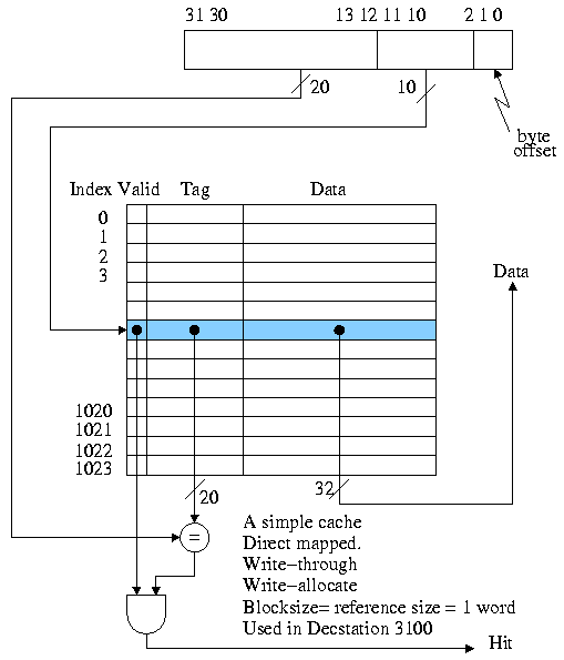
To determine if we have a hit or a miss, and to return the data in
case of a hit is quite easy, as the circuitry indicates.
Make sure you understand the division of the 32 bit address into
20, 10, and 2 bits.
Calculate on the board the total number of bits in this cache and
the number used to hold data.
Homework: Calculate the
total number of bits in the figure 5.8 cache and the number used to
hold data.
Processing a Read for this Simple Cache
The action required for a hit is clear, namely return to the
processor the data found in the cache.
For a miss, the best action is fairly clear, but requires some
thought.
- Clearly we must go to central memory to fetch the requested
data since it is not available in the cache.
- If the cache line was invalid, we store the memory block in
the cache as well as returning it to the processor.
- The question remaining is, assuming the the miss occurred for
a valid line, should we place in the cache the
data fetched from memory, evicting the old data (which was for
a different address), or should we keep the old
data in the cache.
- We definitely want to store the new data instead of
the old.
Question: Why?
Answer: Temporal Locality.
- Question: What should we do with the old data?
Can we just toss it or do we need to write it back to central
memory?
Answer: It depends!
- We will see shortly that the action needed on this
read miss, depends on our choice of action
for a write hit.
Handling Cache Misses
We just need to note a few points.
- The instruction and data memory are replaced with caches.
- On cache misses one needs to fetch/store the desired
datum or instruction from/to central memory.
- This is very slow and hence, in a single cycle implementation,
the cycle time must be very long.
- In a pipelined implementation, the pipeline is stalled while
the cache line is fetched from main memory.
- The above is simplified; considerable effort
is done to avoid many of these stalls..
Handling Writes
Processing a write for our simple cache (direct mapped with block
size = reference size = 1 word).
We have 4 possibilities: For a write hit we must choose between
Write through and Write back.
For a write miss we must choose between write-allocate and
write-no-allocate (also called store-allocate and store-no-allocate
and other names).
Write Hits
We definitely update the cache with the new value and discard the
outdated value previously there (which is now invalid).
Question: Do we update central memory with this new
value?
Answer: It depends!
Write through: Write the data to
memory as well as to the cache.
With a write-through cache policy, both the memory and the cache
are always up-to-date.
Write back: Don't write to memory
now, do it later when this cache block is evicted.
With a write back policy, the cache is always up-to-date, but the
memory can be stale (contain an out-of-date value).
The fact that an eviction must trigger a write to memory for
write-back caches explains the comment above that the write hit
policy effects the read miss policy.
For demand paging, write-back is always used; the cost of
doing the I/O is too large!
Recall that you can have many write hits for separate words on a
page.
For our blksize=refsize=1 cache, this can't happen.
Write Misses
If the write miss was to an invalid line, there is no contention
for the cache block since the block is currently empty (invalid).
The difficulty occurs when the miss is to a valid block (but a
different tag).
In this, more difficult, case two different policies can be
used.
Write-allocate: Write the new data into the
cache (recall we have a write miss).
The handling of the eviction this causes depends on the write hit
policy.
- If the cache is write through, discard the old data
(since it is in memory) and write the new data to memory (as
well as in the cache).
- If the cache is write back, the old data must now be
written back to memory, but the new data is not
written to memory.
Actually (as with demand paging in OS) we keep track of whether
the cache block is clean or dirty and only in the later case is is
sent to memory.
For simplicity, I won't mention this caveat each time we copy-back
a cache line.
Write-no-allocate: Leave the cache alone and
just write the new data to memory.
Normally write-no-allocate is paired with write-through and
write-allocate is paired with write-back.
An Example-Based Summary of the Possible Actions
The basic assumption we have made is what I call blksize=refsize=1,
that is all references are to a word (not a byte) and every cache
block is also 1 word.
(We are also assuming a direct mapped cache, but that will be
explained later when we study associative caches.)
For the following example we assume in addition
- A variable x is stored in memory block 84 (which
equals word 84, which consists of bytes 336-339.)
- Another variable y is stored in memory block
148.
- The cache contains 64 blocks.
Both x and y are assigned to the same cache
block, namely cache block 20, since 84 mod 64 = 20 = 148 mod 64.
The tag associated with x is 84/64 = 1 and the tag
associated with y is 148/64 = 2.
Six Questions
We must consider loads and stores and for each hits
and misses.
I divide the misses into two cases: the block is invalid vs the tag
doesn't match.
- What do we do if we we issue lw x, i.e., read the
cache, and
- the cache access is a hit.
- the cache access is a miss because block 20
is invalid.
- the cache access is a miss
because y not x is stored in block
20 and hence the tags do not match.
- What do we do if we issue sw x, i.e., write the
cache, and
- the cache access is a hit.
- the cache access is a miss because block 20
is invalid.
- the cache access is a miss
because y not x is stored in block
20 and hence the tags do not match.
Answers
For each question we must decide what to return to the processor (if
anything), what do to the cache, and what to do to the memory.
We shall see that some cases are clear; others are not.
- lw x
- (hit) Obvious.
Return to the processor the value (x) found in the
cache; do not alter the cache; do not access memory.
- (miss, invalid) Clear.
Fetch x from memory; store x in the
cache and return x to the processor.
- (miss, wrong tag) Only partially clear.
Clearly we fetch x from memory; return x
to the processor; and (due to temporal locality)
store x in the cache replacing y.
Whether the evicted y must be sent to memory
depends on whether memory is kept up to date (see answers for
2).
- sw x
Since this is a store, we return nothing to the processor.
- (hit) Only partially clear.
Update the cache with the new value of x sent by
the processor, and discard the old value previously cached.
Whether to update memory depends on whether the cache is
write-through (do the update, keeping the memory up to date)
or write-back (do not update, permitting the memory to become
stale).
- (miss, invalid) Not clear at all.
If the cache is write-no-allocate, the cache is not written
but the memory is updated.
If the cache is write-allocate and write-back, the cache is
written but the memory is not.
In the uncommon write-allocate, write-through case both the
cache and memory are written.
- (miss, wrong tag) Not clear at all.
If the cache is write-no-allocate, the cache is unchanged
but x is forwarded to memory.
In the cache is write-allocate, write-back case x
is stored in the cache replacing y, which must be
sent to memory.
In the write-allocate, write-through case x is
stored in the cache and x
but not y is sent to memory,
maintaining the write-through property that memory is always
up-to-date.
Start Lecture #21
The Decstation 3100 Write Policy
The simplest write policy is write-through, write-allocate.
The decstation 3100 discussed above adopted this policy and
performed the following actions for any write, hit or miss, (recall
that, for the 3100, block size = reference size = 1 word and the
cache is direct mapped).
- Index the cache using the correct LOBs (i.e., not the very
lowest order bits as these give the byte offset).
- Write the data and the tag into the cache.
- For a hit, we are overwriting the tag with itself.
- For a miss, we are performing a write allocate and, since
the cache is write-through, memory is guaranteed to be
correct so we can simply overwrite the current entry.
- Set Valid to true (it may already be true).
- Send the request to main memory.
Although the above policy has the advantage of simplicity,
it is out of favor due to its poor performance.
Recall, from last class, the following
Definitions
- A cache hit occurs when a memory reference is found
in the cache.
- A miss is a non-hit.
- The hit rate is the fraction of memory references
that are hits.
- The miss rate is 1 - hit rate, which is the
fraction of references that are misses.
- The hit time is the time required for a hit.
- The miss time is the time required for a miss.
- The miss penalty is miss time - hit time.
Using these definitions we can express quantitatively the
inefficiency of the Decstation 3100.
- For the GCC benchmark, 11% of the operations are stores.
- If we assume an infinite speed central memory (i.e., a
zero miss penalty) or a zero miss rate, the CPI is 1.2 for
some reasonable estimate of instruction speeds.
- Assume a 10 cycle store-miss penalty, which is conservative.
Since the 3100's write-through policy means we have to write main
memory on hits and misses, all writes have this
penalty.
Hence the CPI becomes 1.2 + 11% * 10 = 2.3, which is half
speed.
- Today the penalty would be more like 100 than 10 so the CPI
would be 1.2 + 11% * 100 = 12.2, which is 1/10 speed!
Improvement: Use a Write Buffer
- Hold a few writes at the processor while they are being
processed at memory.
- As soon as the word is written into the write buffer, the
instruction is considered complete and the next instruction can
begin.
- Hence the write penalty is eliminated as long as the word can be
written into the write buffer.
- Must stall (i.e., incur a write penalty) if the write buffer is
full.
This occurs if a bunch of writes occur in a short period.
- If the rate of writes is greater than the rate at which memory
can handle writes, you must stall eventually.
The purpose of a write-buffer (indeed of buffers in general) is to
handle short bursts.
- The Decstation 3100 (which employed the simple cache structure
just described) had a 4-word write buffer.
- Note that a read miss checks the write buffer.
Unified vs Split I and D (Instruction and Data) Caches
In order to increase the bandwidth to memory, modern computers
normally employ two caches, one for the instruction memory and one
for the data memory.
Naturally, a system with both a 1MB instruction cache and a 1MB data
cache performs better than a system with just a single
1MB unified
cache used for both instructions and data.
The real question is, given a fixed total size (in bytes) for the
cache, is it better to have two caches, one for instructions and one
for data; or is it better to have a single unified cache?
- Unified is better because it automatically performs
load balancing
.
If the current program needs more data references than
instruction references, the cache will accommodate.
Similarly if more instruction references are needed.
- Split is better because it can do two references at once (one
instruction reference and one data reference).
- The winner is ...
split I and D (at least for L1).
- But unified has the better (i.e. higher) hit ratio.
- So hit ratio is not the ultimate measure of
good cache performance.
Improvement: Multiword Blocks
The setup we have described does not take any advantage of spatial
locality.
The idea of having a multiword block size is to bring into the cache
words near the referenced word since, by spatial locality, they are
likely to be referenced in the near future.
We continue to assume (for a while) that the cache is direct mapped
and that all references are for one word.
The book's terminology for byte offset
and block
offset
is inconsistent.
The byte offset gives the offset
of the byte within the word so the
offset of the word within the block should be
called the word offset, but alas it is called the block offset in
the 2e, 3e, and 4e.
I don't know if this is standard terminology or a long standing typo
in all three editions.
I wrote to Patterson, who basically agreed, but the terminology is
unchanged in 5e..
I will try to use the longer but clearer term word-in-block
for the offset of the word in the block.
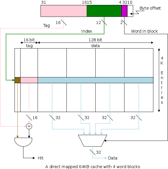
The figure on the right shows a 64KB direct mapped cache with
4-word (16-byte) blocks.
Questions: For this cache, when the memory word
referenced is in a given block, where in the cache does the block
go, and how do we find that block in the cache?
Answers:
- Byte n is in word n/4,
for the 4-byte words we are assuming.
So bytes 4n...4n+3 are in word n.
- For a cache like the one on the right with 16B (4 word) blocks,
byte n is stored in the memory
block n/16 and word n is stored in memory
block n/4.
So bytes 16n...16n+15 are stored in
block n.
- The word-in-block = the word address modulo 4 (the number of
words per block).
- The number of blocks in the cache = the size of the cache
divided by the size of each block.
For the pictured cache this is 64KB / 16B = 4K.
- The cache block number or cache line number =
the memory block number modulo the number of blocks in the
cache (for the direct mapped caches we are now studying).
- The tag = the memory block number / the number of blocks in the
cache.
Show from the diagram how this gives the pink portion for the tag
and the green portion for the index or cache block number.
Consider the cache shown in the diagram above and a reference to
word 17003.
- 17003 / 4 = 4250 with a remainder of 3.
Hence the memory block number is 4250 and the word-in-block is
3.
- A 64KB cache with 16B blocks has 64KB/16B=4K=4096 entries.
Since 4250 / 4096 gives 1 with a remainder of 154, memory block
number 4250 is stored in cache line 154 with a tag of 1.
Summary: Memory word 17003 resides in word 3 of
cache block 154 with tag 154 set to 1 and with valid 154 true.
The cache size or cache capacity is
the size of the data portion of the cache (normally measured in
bytes).
For the caches we have see so far this is the block size times the
number of entries.
For the diagram above this is 64KB.
For the simpler direct mapped caches block size = word size so the
cache size is the word size times the number of entries.
Note that the total size of the cache includes all the bits.
Everything except for the data portion is considered overhead since
it is not part of the running program.
For the caches we have see so far the total size is
(block size + tag size + 1) * the number of entries
Let's compare the pictured cache with another one containing 64KB
of data, but with one word blocks.
- Calculate on the board the total number of bits in each cache;
this is not simply 8 times the cache size in
bytes.
- If the references are strictly sequential the pictured cache
has 75% hits; the simpler cache with one word blocks
has no hits.
Homework: 5.3.1 and
5.3.2, and 5.3.3.
How do we process read/write hits/misses for a cache with multiword
blocks?
- Read hit: As before, return the data found to the
processor.
- Read miss: As before, due to locality we discard (or write back
depending on the write hit policy) the old line and fetch the new
line.
- Write hit: As before, write the word in the cache (and perhaps
write memory as well depending on the policy).
- Write miss: A new consideration arises.
As before we might or might not decide to replace the current
line with the referenced line and, if we do decide to replace
the line, we might or might not have to write the old line back.
The new consideration is that if we decide to replace the line
(i.e., if we are implementing store-allocate), we must remember
that we only have a new word and the unit of
cache transfer is a multiword line.
- The simplest idea is to fetch the entire old line and
overwrite the new word.
This is called write-fetch and is something
you wouldn't even consider with block size = reference size =
1 word.
Why?
Answer: You would be fetching the one word that you want to
replace so you would fetch and then discard the entire
fetched line.
- Why, with multiword blocks, do we fetch the whole line
including the word we are going to overwrite?
Answer.
The memory subsystem probably can't fetch just words
1,2, and 4 of the line.
- Why might we want store-allocate and
write-no-fetch?
Answer Because a common case is storing consecutive words:
With store-no-allocate all are misses and with
write-fetch, each store fetches the line to
overwrite another part of it.
- To implement store-allocate-no-write-fetch (SANF), we need
to keep a valid bit per word.
Why not make block size enormous?
For example, why not have the cache
be one huge block.
- NOT all access are sequential.
- With too few blocks misses go up again.
Start Lecture #22
Memory Support for Wider Blocks
Recall that our processor fetches one word at a time and our memory
produces one word per request.
With a large block size cache, the processor still requests one word
and the cache still responds with one word.
However the cache requests a multiword block from memory and to date
our memory is only able to respond with a single word.
The question is, "Which pieces and buses should be narrow (one word)
and which ones should be wide (a full block)?".
The same question arises when the cache requests that the memory
store a block and the answers are the same so we will only consider
the case of reading the memory.
Since the processor is only requesting a single word, a wide bus
between the cache and processor seems silly.
The processor would then need a mux to discard the other
words.
One could imagine a buffer to store the entire block acting as a
kind of L0 cache, but this would not be so useful if the L1 cache
was fast enough).
The question we now want to consider is whether the memory should be
wide.
That is, should the memory have enough pins and the bus enough
enough wires so that the entire block can be transferred at
once.
We make the following timing assumptions.
- Only 1 cycle is required to send the address.
This is valid since only one address is needed per access for
all designs.
- 15 clocks are required for each memory access (independent of
width).
Today the number would likely be bigger than 15 (since processor
cycle times have improved faster that memory access times), but it
would remain independent of the width.
- 1 Clock is required to transfer each busload of data.
Consider the three designs shown on the right.
The left one assumes the memory delivers one word at a time and the
bus is 1-word wide.
This is the most economical design.
The middle design has a wide memory that can deliver an entire
(4-word) block at one time and has a block-wide bus that can deliver
the entire block to the cache in one cycle.
This is the most luxurious design.
Since the processor requested only one word, presenting the wide
interface to the processor is not helpful and would not appear in
practice.
The rightmost design has four word-wide memories that are
interleaved and thus can together produce a 4-word block at one
time.
However, the bus can only deliver one word at a time to the cache.
The question is how long does it take to satisfy a read miss for
the cache above and each of the three memory/bus systems.
- The narrow design takes 65 cycles: 1 address transfer, 4 memory
reads, 4 data transfers.
One could do a little better by starting the second access to
memory the same cycle you transfer the first word back to the
cache.
This is a form of pipelining.
- The wide design (b) takes 17.
- The interleaved design (c) takes 20.
Interleaving works well here because in this case we are
guaranteed to have sequential accesses.
Imagine a design between (a) and (b) with a 2-word wide
datapath.
It takes 33 cycles and is more expensive to build than (c).
Homework: Assume the
block size is 8 words.
How long would an access take for a narrow, wide, and interleaved
design?
How long for a 2-word wide design and for a 4-word design.
5.4: Measuring and Improving Cache Performance
I added interludes last year since I realized that CS students
have little experience in these performance calculations.
I may include the interludes several times.
Interlude on Solving Rate and Time Equations
- A cycle (or clock cycle) is the time for the
clock to go from one active edge to the next active edge.
- Herz means CPS, i.e., cycles per second.
It is a rate (like MPH) not a
time.
So a clock rate of 50 Hz means 50 cycles per second, which also
means 50 cycles = 1 second or 1 cycle = 1/50 second.
- Continuing with the same example 1 cycle = 2*10-2
sec. = 20*10-3 sec. = 20ms = 20,000*10-6 sec
= 20,000us = 20*106*10-9 =
20 million ns.
- KHz is kilohertz = 1,000Hz.
MHz is megahertz = 106Hz; GHz is gigahertz =
109Hz.
- Question: Which takes longer 1GHz or
10MHz?
Answer: Nonsense!
Hz is rate NOT time.
- Question: Which takes longer one cycle at 1GHz
or one cycle at 10MHz
Answer: 1GHz means 109 cycles = 1
sec; so 1 cycle = 10-9 sec.
10MHz means 10*106 cycles = 1 sec; so 1 cycle =
0.1*10-6 sec = 10-7 sec.
So a cycle at 10MHz takes 100 times as long as a cycle at
1GHz.
- Question: At a rate of 2GHz, how long is one
cycle?
Answer: 2GHz means 2*109 cycles = 1
second.
Hence 1 cycle = 0.5*10-9sec = 0.5ns
- Question: What megahertz clock has a 300ns
cycle time?
Answer: 300ns cycle time means 1 cycle = 300ns =
300*10-9 sec.
So 1 sec = (1/300)*109 cycles = (10/3)*106
cycles = 3.33MHz.
Interlude on Averages Given Base Plus Extra
- Question: In
2/5 of the cases X=A, in 3/5 of the cases X=B.
What is the average X?
Answer: (2A + 3B) / 5
- Question:
30% of cases X=A; the rest X=B.
What is the average X?
Answer: Average X =(30/100)A + (70/100)B
- Question:
p% X=A; rest X=B.
What is the average X?
Answer:
Average X = (p/100)A + ((100-p)/100)B
- Question:
p% X=A+E; rest X=A (E stands for extra).
What is the average X?
Answer:
Average X = (p/100)(A+E) + ((100-p)/100)A
= (p/100)A + (p/100)E + ((100-p)/100)A
= (100/100)A + (p/100)E = A + (p/100)E
- Question:
Base cost is 13; 17% of the cases have an extra cost of E.
What is the average cost?
Answer:
Average cost = 13 + (17/100)E = 13 + .17E
- Question:
Base CPI = 13; 17% of refs miss cache with a penalty of 8 cycles.
What is the overall CPI?
Answer:
Overall CPI = 13 + .17(8) = 14.36 cycles.
An Example
We assume separate instruction and data caches (split I and D).
But if both caches have a miss, the misses are processed one at a
time because there is only one central memory (remember that the
instruction and data memories of our MIPS datapath correspond to
caches in a real machine.
Do the following performance example on the board.
It would be an appropriate final exam question.
- Assume
- 5% I-cache misses.
- 10% D-cache misses.
- 1/3 of the instructions access data.
- The CPI = 4 if there are no cache misses.
This (unrealistic) situation is sometimes called
the base CPI.
- What is the CPI if the miss penalty is 12 cycles?
- What is the CPI if we upgrade to a double speed cpu+cache, but
keep a single speed memory (i.e., a 24 cycle miss penalty)?
- How much faster is the
double speed
machine?
It would be double speed if there was a 0% miss rate.
A lower base (i.e. miss-free) CPI makes stalls appear more
expensive since waiting a fixed amount of time for the
memory corresponds to losing more instructions if the CPI
is lower.
A faster CPU (i.e., a faster clock) makes stalls appear more
expensive since waiting a fixed amount of time for the memory
corresponds to more cycles if the clock is faster (and hence more
instructions since the base CPI is the same).
Another performance example.
- Assume
- I-cache miss rate 3%.
- D-cache miss rate 5%.
- 40% of instructions reference data.
- miss penalty of 50 cycles.
- Base CPI is 2.
- What is the CPI including the misses?
- How much slower is the machine when misses are taken into account?
- Redo the above if the I-miss penalty is reduced to 10 (D-miss
still 50)
- With I-miss penalty back to 50, what is performance if CPU (and the
caches) are 100 times faster
Homework:
Consider a system that has a miss-free CPI of 2, a D-cache miss rate
of 5%, an I-cache miss rate of 2%, has 1/3 of the instructions
referencing memory, and has a memory that gives a miss penalty of 20
cycles.
The clock speed stays the same throughout this problem.
- What is the CPI?
- What would be the CPI if the memory was double speed, but
the CPU+caches remained the same as the original?
- What would be the CPI if the memory remained the same as the
original but the CPU+cache were double speed.
- How fast would the CPU+cache have to be so that the system
was twice as fast as the original, with the original memory?
Note:
Larger caches typically have higher hit rates but
longer hit times.
Start Lecture #23
Remark: The final is NOT in this room.
According to https://cs.nyu.edu/dynamic/courses/exams.
The final is 4PM thurs 21 dec in Tisch LC13.
Is that room easy to find?
Reducing Cache Misses by More Flexible Placement of Blocks
Improvement: Associative Caches
Consider the following sad story.
Jane's computer has a cache that holds 1000 blocks and Jane has a
program that only references 4 (memory) blocks, namely blocks 23,
1023, 123023, and 7023.
In fact the references occur in order: 23, 1023, 123023, 7023, 23,
1023, 123023, 7023, 23, 1023, 123023, 7023, 23, 1023, 123023, 7023,
etc.
Referencing only 4 blocks and having room for 1000 in her cache,
Jane expected an extremely high hit rate for her program.
In fact, the hit rate was zero.
She was so sad, she gave up her job as web-mistress, went to medical
school, and is now a brain surgeon at the mayo clinic in Rochester
MN.
So far we have studied only direct mapped caches,
i.e., those for which the location in the cache
is determined by the address.
Since there is only one possible location in the cache for any
block, to check for a hit we compare one tag with
the HOBs of the addr.
The other extreme is a fully associative cache.
- A memory block can be placed in any cache block.
- Since any memory block can be in any cache block, the cache
index where the memory block is stored tells us nothing about
which memory block is stored there.
Hence the tag must be the entire memory block number
Moreover, we don't know which cache block to check so we must
check all cache blocks to see if we have a hit.
- The larger tag is a problem.
- The search is a disaster.
- It could be done sequentially (one cache block at a time),
but this is much too slow.
- We could have a comparator with each tag
and mux all the blocks to select the one that matches.
- This is too big due to both the many comparators and
the humongous mux.
- However, it is exactly what is done when implementing
translation lookaside buffers (TLBs), which are used with
demand paging.
- Question: Are the TLB designers
magicians?
Answer: No, TLBs are small.
- An alternative is to have a table with one entry per
memory block telling if the memory block is in
the cache and if so giving the cache block number.
This is too big and too slow for caches but is exactly what is
used for demand paging (recall 202) where the memory blocks in 436
correspond to pages on disk in 202 and the table we would need in
436 is called the page table in 202.
Set Associative Caches
Most common for caches is an intermediate
configuration called set associative or n-way associative
(e.g., 4-way associative).
The value of n is typically a small power of 2.
If the cache has B blocks, we group them into B/n
sets each of size n.
Since an n-way associative cache has sets of size n blocks,
it is often called a set size n cache.
For example, you often hear of set size 4 caches.
In a set size n cache,
memory block number K is stored in set K mod the number of sets,
which equals K mod (B/n).
The picture below shows a system storing memory block 12 in three
cache, each having 8 blocks.
The left cache is direct mapped; the middle one is 2-way set
associative; and the right one is fully associative.
- The blue (both light and dark) indicate the cache blocks in
which memory block 12 might have been
stored.
- The dark blue is the cache block in which the memory block 12
is stored.
- The arrows show the blocks (i.e., tags) that must be searched
to look for memory block 12.
The arrows point to the blue blocks.
- The corresponding figure in the book (5.14) has Tag=12 for all
three caches.
Our figure corrects this typo.
Direct Mapped Caches
We have already done direct mapped caches but to repeat:
- The cache block number containing a memory block equals the
memory block number mod the number of cache blocks.
- Expressed algebraically: CBN = MBN mod NCB.
- Similarly, the tag = MBN / NCB.
- In the example, the memory block number is 12 and there are 8
cache blocks so memory block 12 is stored in cache block 12 mod 8
= 4 and the tag is 12 / 8 = 1.
Set Associative Caches
The middle picture shows a 2-way set associative
cache also called a set size 2 cache.
A set is a group of consecutive cache blocks.
- As the name indicates the size of each set in the picture is 2
(cache blocks) and hence the number of sets = the number of cache
blocks / 2.
- Algebraically: NS = NCB / SS.
- A memory block is stored in a set (technically in one of the
cache blocks of the set).
Specifically, the set number is the memory block number mod the
number of sets, which equals the memory block number mod (the
number of cache blocks / the size of each set).
- Algebraically: SN = MBN mod NS = MBN / mod (NCB / SS).
- Similarly, in a 2-way set-associative cache, the tag stored
equals the memory block number / the number of sets.
- In the example memory block 12 is stored in cache set
12 mod (8/2) = 12 mod 4 = 0.
- Similarly, the tag is 12/(8/2) = 3.
- We do not know which (if any) of the cache
blocks in the set contain the memory.
Hence we must check the tags for all entries in the set to see if
any match.
This explains the two arrows in the middle diagram.
Fully Associative Caches
The right picture shows a fully associative cache, i.e. a cache
where there is only one set and it is the entire cache.
- In the example the one set has 8 elements so memory block 12 is
stored in set 12 mod (8/8) = 12 mod 1 = 0, which is the only
set.
- The tag is 12 / (8/8) = 12/1 = 12, i.e., the entire memory block
number
- We do not know which (if any) of the cache
blocks in the set contain the memory.
Hence we must check the tags for all entries in the entire cache
to see if any match.
This explains the eight arrows in the right diagram.
- These three points hold for fully associative caches of any
size.
For a cache holding n blocks, a set-size n cache is
fully associative and a set-size 1 cache is direct
mapped.
Do the same example in class for a 4-way set associative cache.
Determining the Set Number and the Tag
Recall that for the a direct-mapped cache, the cache
index is the cache block number (i.e., the cache is indexed by cache
block number).
For a set-associative cache, the cache index is the set
number.
Just as the cache block number for a direct-mapped cache is the
memory block number mod the number of blocks in the cache, the set
number for a set-associative cache is the (memory) block number mod
the number of sets.
Just as the tag for a direct mapped cache is the memory block
number divided by the number of blocks, the tag for a
set-associative cache is the memory block number divided by the
number of sets.
Summary: Divide the memory block number by the
number of sets in the cache.
The quotient is the tag and the remainder is the set number.
(The quotient is normally referred to as the memory block number mod
the number of sets.)
Do NOT make the mistake of thinking that a set
size 2 cache has 2 sets, it has NCB/2 sets each of size 2.
Ask in class.
- What is another name for an 8-way associative cache having 8
blocks?
- What is another name for a 1-way set associative cache?
Question: Why is set associativity good?
For example, why is 2-way set associativity better than direct
mapped?
Answer: Consider referencing two arrays of size 50K
that start at location 1MB and 2MB.
- Both contend for the same cache blocks in a direct mapped 128KB
cache.
- They fit together in a 128K 2-way associative cache.
Locating a Block in the Cache
Question: How do we find a memory block in a 4KB
4-way set associative cache with block size 1 word?
Answer: This is more complicated than for a
comparable direct mapped cache.
We proceeds as follows.
- First drop the low 2 bits (byte in word) of the memory address,
leaving 30 bits for the memory word number (MWN).
- The MBN = the MWN since, in this example, the block size is 1
word.
- Each set contains 4 blocks = 4 words = 16B.
- Hence the cache has 4KB/16B=256 sets
- Divide the memory block number by the number of sets.
The quotient is the tag.
That is, tag = MBN / NS = MBN / 256.
Since 256=28, dividing by 256 is simply simply
separating the dividend into two pieces: the left 8 bits are the
remainder and the rest is the quotient.
- The quotient, i.e, the tag, shown in pink in the diagram.
- The remainder (i.e., the memory block number mod the number of
sets) is the set number (i.e., the index of the entry).
This portion of the address is shown in green.
- Compare all the tags and valid bits in the set
with the tag of the memory block.
- If any valid tag matches, a hit has occurred
and the corresponding data entry contains the memory block.
- If no valid tag matches, a miss has
occurred.
The advantage of increased associativity is normally an increased
hit ratio.
Question: What are the disadvantages?
Answer: It is slower, bigger, and uses more energy
due to the extra logic.
Combining Set-Associativity and Multiword Blocks
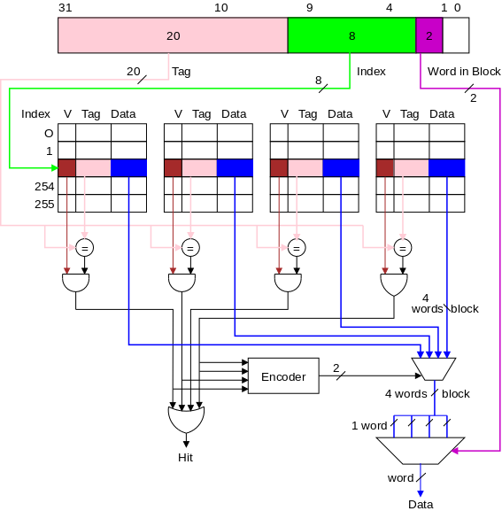
This is a fairly simple combination of the two ideas and is
illustrated by the diagram on the right.
- Start with the picture just above for a set-associative,
blocksize = 1 word, cache.
- Each blue portion of the cache is now a multi-word block, not
just a single word.
- Hence the
data
coming out of the multiplexor at
the bottom right of the previous is now a block.
In the diagram on the right, the block is 4 words.
- As with direct-mapped caches having multi-word blocks, we again
use the word-within-block bits to choose the proper word.
In the diagram this is performed by the very bottom multiplexor,
using the magenta word-within-block bits as the selector
line.
Our description and picture of multi-word block, direct-mapped
caches is here, and our description
and picture of single-word block, set-associative caches is just
above.
It is useful to compare those two picture with the one on the right
to see how the concepts are combined.
Below we give a more detailed
discussion of which bits of the memory address are used for which
purpose in all the various caches.
Choosing Which Block to Replace
When an existing block must be replaced, which victim should we
choose?
We asked the exact same question (using different words) when we
studied demand paging in 202.
- The victim must be in the same set (i.e., have the same index)
as the new block.
With direct mapped (a.k.a 1-way associative) caches, this
determines the victim so the question doesn't arise.
- With a fully associative cache all resident blocks are
candidate victims.
This is exactly the situation for demand paging (with global
replacement policies) and is also the case for
(fully-associative) TLBs.
- Random replacement is sometimes used for caches, i.e., choose a
random block in the set to be the victim.
- This is never done for demand paging.
A demand paging system spends extra time
on misses to do a better job (i.e., get a
higher hit rate).
- For caches, speed is crucial so we have no time for
calculations, even for misses.
- LRU is much better than random, but is cannot
be done quickly enough for caches (or for pages).
- If the cache is 2-way set associative, each set is of size
two and it is easy to quickly find which of the two blocks is
lru.
Question: How?
Answer: For each set keep a bit indicating
which block in the set was just referenced and the lru block
is the other one.
- If the cache iS 4-way set associative, each set is of size
4.
Consider these 4 blocks as two groups of 2.
Use the trick above to find the group most recently used and
pick the other group.
Then use the trick again within the lru group and chose the
lru block in that group.
- Sound great.
We can do lru fast for any power of two using a binary tree.
- Question: Why didn't the OS (demand paging)
designers think of this?
Was it because ...
- OS designers are not as smart as cache designers.
- OS designers can't require a power of two pages.
- This scheme does not work.
Answer: C.
- The above is not LRU; it is just an approximation.
Show this on the board.
Start Lecture #24
How Big
Is a Cache?
There are two notions of size.
Definition: The cache size
is the capacity of the cache.
- This means, the total size of all the blocks.
- In the diagrams above it is the size of the blue portions.
- The size of the cache in the last diagram is 256 * 4 * 16B =
16KB.
- The size of the cache in the previous diagram is 256 * 4 * 4B =
4KB.
- So you should not compare the performance of these two; of
course the bigger cache will do better.
- Instead the second cache should be reduced to 64 sets or the
first increased to 1024 sets.
Another size of interest is the total number of
bits in the cache, which includes tags and valid bits.
For the 4-way associative, 1-word per block cache shown above, this
size is computed as follows.
- The 32 address bits contain 8 bits of index and 2 bits
giving the byte offset.
- So the tag is 22 bits (more examples just below).
- Each cache entry contains 1 valid bit, 22 tag bits and 32 data
bits, for a total of 55 bits.
- There are 256*4=1K entries.
- So the total size is 55Kb (kilobits).
For this cache, what fraction of the bits are user data?
Ans: 4KB / 55Kb = 32Kb / 55Kb = 32/55.
Calculate in class the equivalent fraction for the last diagrammed
cache, having 4-word blocks (and still 4-way set associative).
Tag Size and Division of the Address Bits
We continue to assume a byte addressed machines with all references
to a 4-byte word.
The 2 LOBs are not used (they specify the byte within the word, but
all our references are for a complete word).
We show these two bits in white.
We continue to assume 32-bit addresses so there are 230
words in the address space.
Let us review various possible cache organizations and determine
for each the tag size and how the various address bits are used.
We will consider four configurations each a 16KB cache.
That is the size of the data portion of the cache
is 16KB = 4 kilowords = 212 words.
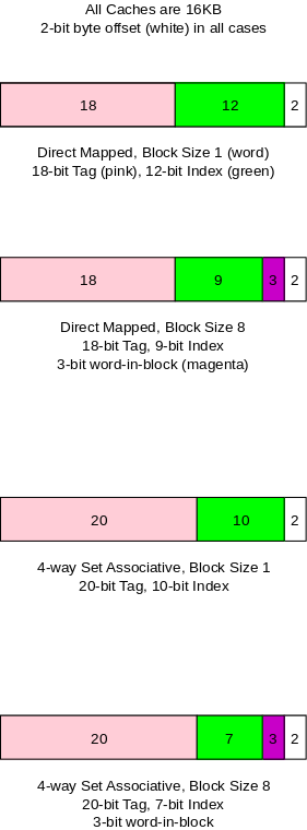
Direct Mapped, Block Size 1 (Word)
This is the simplest cache.
- Since the block size is one word, there are 230 memory
blocks and all the address bits (except the white 2 LOBs that
specify the byte within the word) are used for the memory block
number.
Specifically, 30 bits are so used.
- Any 16KB cache contains 214 bytes = 212
words, which, for this direct mapped, blocksize=wordsize cache,
is 212 blocks = 212 sets.
- Divide the MBN by NS.
The remainder, i.e., the low order 12 bits of the MBR gives the
index in the cache (the CBN), shown in green.
- The quotient (the remaining 30-12=18 bits) is the tag, shown
in pink.
Direct Mapped, Block Size 8
Modestly increasing the block size is an easy way to
take advantage of spacial locality.
- Three bits of the address give the word within the 8-word block.
These bits are shown in magenta.
- The remaining 27 HOBs of the memory address give the memory
block number.
- The cache still has 212 words, but this is now only
29 blocks = 29 sets.
- So the low order 9 bits of the MBN is the CBN, which is the
index in the cache.
- The remaining 27-9=18 bits are the tag.
4-Way Set Associative, Block Size 1
Increasing associativity improves the hit rate but
only a modest associativity is practical.
- The block size is back to 1 word so there are 230
memory blocks and the MBN is again 30 bits.
- The cache has 212 words = 212 blocks =
210 sets (each set has 4=22 blocks).
- So the low order 10 bits of the memory block number gives the
index in the cache.
- The remaining 20 bits are the tag.
- As the associativity grows, the tag gets bigger.
Question: Why?
Answer: Growing associativity reduces the number
of sets into which a block can be placed, which increases the
number of memory blocks eligible to be placed in a given set.
Hence more bits are needed to see if the desired block is
there.
4-Way Set Associative, Block Size 8
The two previous improvements are often combined.
- Three bits of the address give the word within the block.
- The remaining 27 HOBs of the memory address give the memory
block number.
- The cache has 212 words = 29 blocks =
27 sets.
- So the low order 7 bits of the memory block number give the
index in the cache.
- The remaining 20 bits form the tag.
On the board calculate, for each of the four caches, the memory
overhead percentage.
Homework: Redo the four
caches above with the size of the cache increased from 16KB to 64KB
determining the number of bits in each portion of the address as
well as the overhead percentages.
Reducing the Miss Penalty Using Multilevel Caches
Improvement: Multilevel caches
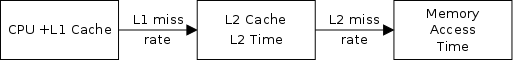
Modern high end PCs and all servers all have at least two levels
of caches: A very fast, and hence not very big, first level (L1) cache
together with a larger but slower L2 cache.
When a miss occurs in L1, L2 is examined and only if a miss occurs
there is main memory referenced.
So the average miss penalty for an L1 miss is
  (L2 hit rate)*(L2 time) + (L2 miss rate)*(L2 time + memory time) =
  (l2 time) + (L2 miss rate) * (memory time)
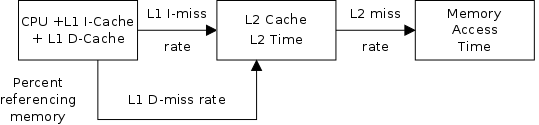
The situation is more complicated than the above diagram and
formula indicate since, as we have seen before, there are L1
I-caches and L1 D-caches, each of which can independently experience
misses.
We need the diagram on the right; the corresponding formula is
below.
The bottom U-shaped arrow in that diagram corresponds to data
references, which occur only for load/store type instructions.
Interlude on Solving Rate and Time Equations (repeat)
- A cycle (or clock cycle) is the time for the
clock to go from one active edge to the next active edge.
- Herz means CPS, i.e., cycles per second.
It is a rate (like MPH) not a
time.
So a clock rate of 50 Hz means 50 cycles per second, which also
means 50 cycles = 1 second or 1 cycle = 1/50 second.
- Continuing with the same example 1 cycle = 2*10-2
sec. = 20*10-3 sec. = 20ms = 20,000*10-6 sec
= 20,000us = 20*106*10-9 =
20 million ns.
- KHz is kilohertz = 1,000Hz.
MHz is megahertz = 106Hz; GHz is gigahertz =
109Hz.
- Question: Which takes longer 1GHz or
10MHz?
Answer: Nonsense!
Hz is rate NOT time.
- Question: Which takes longer one cycle at 1GHz
or one cycle at 10MHz
Answer: 1GHz means 109 cycles = 1
sec; so 1 cycle = 10-9 sec.
10MHz means 10*106 cycles = 1 sec; so 1 cycle =
0.1*10-6 sec = 10-7 sec.
So a cycle at 10MHz takes 100 times as long as a cycle at
1GHz.
- Question: At a rate of 2GHz, how long is one
cycle?
Answer: 2GHz means 2*109 cycles = 1
second.
Hence 1 second = 0.5*10-9sec = 0.5ns
- Question: What megahertz clock has a 300ns
cycle time?
Answer: 300ns cycle time means 1 cycle = 300ns =
300*10-9 sec.
So 1 sec = (1/300)*109 cycles = (10/3)*106
cycles = 3.33MHz.
Interlude on Averages Given Base Plus Extra (repeat)
- Question: In
2/5 of the cases X=A, in 3/5 of the cases X=B.
What is the average X?
Answer: (2A + 3B) / 5
- Question:
30% of cases X=A; the rest X=B.
What is the average X?
Answer: Average X =(30/100)A + (70/100)B
- Question:
p% X=A; rest X=B.
What is the average X?
Answer:
Average X = (p/100)A + ((100-p)/100)B
- Question:
p% X=A+E; rest X=A (E stands for extra).
What is the average X?
Answer:
Average X = (p/100)(A+E) + ((100-p)/100)A
= (p/100)A + (p/100)E + ((100-p)/100)A
= (100/100)A + (p/100)E = A + (p/100)E
- Question:
Base cost is 13; 17% of the cases have an extra cost of 8.
What is the average cost?
Answer:
Average cost = 13 + (17/100)8 = 13 + 1.36 = 14.36
- Question:
Base CPI = 13; 17% of refs miss cache with a penalty of 8 cycles.
What is the overall CPI?
Answer:
Overall CPI = 13 + .17(8) = 14.36 cycles.
Interlude on Average Extra Time with Zero, One, or Two Delays
(new)
- If it always takes 30 minutes for me to walk to the end of the
block, then the average time is clearly 30 minutes.
- Now assume 1/4 of the time Ms. Hampton stops me for a 5 minute
chat?
How long is the average walk?
Average time = 30 min + (1/4) 5 min = 31.25 min.
- Now assume 10% of the times we chat, she brings out something
yummy that takes me an extra 20 minutes to eat.
Average time = 30 min + (1/4) 5 min + (1/4)(0.1) 20 min = 31.25
min + 0.025*20 min = (31.25+0.5) min = 31.75 min.
- Call my 30 minute walk the Base CPI, replace
talk to Ms. Hapmton for 5 minutes
with
there is an L1 cache miss with penalty 5 minutes
.
- Similarly, the
yummy
corresponds to an L2 miss.
- To get the analog to separate I and D L1 caches add to the story
that, in addition to Ms. Hampton (who becomes the L1-I Cache
Miss), in 25% of my walks, I am so happy that I whistle (reference
data) and 10% of the whistles cause Ms. Jones to speak to me for 3
minutes (the L1-D cache miss).
As with Ms. Hampton, Ms. Jones has a 10% chance of giving me a
yummy that takes 20 minutes to eat (the L2 D-cache miss).
Solving Problems
Assumptions
We will make five assumptions.
- The system has two L1 caches, an L1 I-cache and an L1 D-cache.
That is how our MIPS datapath is organized.
- The system either has no L2 cache or a single unified L2 cache.
It does not have separate L2 instruction and data
caches.
- The base time is the time for an instruction that hits in both
L1 caches.
We do not separate CPU time from L1 hit time, the CPU processing
includes trying the LI caches.
- If there is an L2, the same L2 time is incurred for both an L2
hit and an L2 miss.
This means that on an L2 miss the memory access begins
after the L2 has determined that the reference is a
miss.
- The system has no L3 or higher caches.
The Instruction Time
For most problems the main job is to find the
instruction time, i.e., the time required to execute one
instruction.
From this time one can easily find, for example, the MIPS rating.
Typically the time is the sum of a base time, which assumes no L1
cache misses (neither I nor D) and some penalties due to possible
cache misses.
(When there are no L1 misses there are no L2 references hence no L2
misses, or L3, L4, ...).
Calculating the base time depends on the specific problem.
One common case is that you are given the base CPI which you then
convert to time per instruction by multiplying by the cycle
time.
The Main Formulas
The following formula makes the assumptions listed
above.
We write Penalty to abbreviate
L1 Miss Penalty.
  Time for one instruction =
     BaseTime + (L1 I-cache miss rate) * Penalty
              + (Prob Inst refs mem) * (L1 D-cache miss rate) * Penalty

  BaseTime =
     BaseCPI * CycleTime

  Penalty =
     if there is an L2 cache
         L2 time + (L2 miss rate) * (Memory Access time)
     else // no L2 cache
         (Memory access time)
The Assumptions Revisited
- Assumption 1 is nearly universally satisfied by today's systems.
We would need to rethink our analysis for a unified (or
nonexistent) L1 cache.
At least we would need to adjust the base CPI to account for the
inability to access the I and D caches simultaneously.
This inability would be a structural hazard to the pipelining we
have assumed
- To analyze a split I and D L2 cache, we would need two
Penalty
terms above, one for instructions and
one for data.
A more significant change would be to notice that the two
penalties could be overlapped at least partially since they are
starting at separate L2 caches.
- One could imagine beginning the L2 access before determining if
the L1 access would be a hit.
We will not do this; I don't believe real systems do it
either.
- If the memory access starts while the L2 is processing, we
would change the then arm by replacing
(Memory Access Time) with
(Memory Access Time - L2Time)
- An L3 cache would mean that the
memory access time
in the
penalty would need to account for the intervening L3 access.
Similarly, for L4, etc.
Start Lecture #25
Remark: The last lab is posted. Note that all
labs must be submitted by 15 dec.
They will not be accepted after that date.
Please try to do it earlier for the grader's (and hence my) sake.
Example 1
Do this example on the board (a reasonably exam
question, but too long as written, since it has so many parts).
Assume
- L1 I-cache miss rate 4%
- L1 D-cache miss rate 5%
- 40% of instructions reference data
- L2 miss rate 6%
- L2 time of 15ns
- Memory access time 100ns
- Base CPI of 2
- Clock rate 400MHz
Calculate
- (Perfect Caches) How many instructions per second would this
machine execute if both L1 caches had a 0% miss rate?
- (No Caches) How many instructions per second would this machine
execute if all caches were eliminated?
- (Normal L1; No L2) How many instructions per second would this
machine execute if the L2 cache was eliminated (L1 as originally
specified)?
- (Normal L1; Perfect L2) How many instructions per second would
this machine execute if the L2 cache had a 0% miss rate (L1 as
originally specified)?
- (Normal L1; Normal L2) How many instructions per second does
this machine execute as originally specified?
Solution.
As always the time for one instruction is
base time + probability of L1 I-miss ×
penalty
+ (probability instruction referenced memory) ×
probability of L1 D-miss × penalty.
A 400MH clock rate implies a 2.5ns cycle time.
Since the base CPI is 2, the base time for an instruction is
5ns.
- A perfect L1 implies the penalty is 0.
Hence 1 instruction takes 5×10⁻⁹ second.
Therefore, in one second, the machine executes 0.5×10⁹
instructions, which is 200MIPS.
- With no caches the time for one instruction is
5ns + Penalty +
(Probability instruction references memory) × Penalty
The penalty = 100ns.
So the time for 1 instruction is
5ns + 100ns + 0.4×100ns = 145ns.
Hence 109 instructions take 145 seconds and the machine
executes 109/145 instructions per seconds or about
7MIPS.
- With no L2 the time for one instruction is
5ns + (4%)100ns + (40%)(5%)100ns = 11ns
This gives 109/11 IPS or about 9MIPS.
- With a perfect L2 the time for one instruction is
5ns + 4%(15ns) + 40%(5%)15ns = 5.9ns
This gives 109/5.9 IPS or about 17MIPS.
- For the original specification the time for one instruction
is
5ns + 4%(15ns + (6%)100ns) + 40%(5%)(15ns + (6%)100ns) =
5ns + .04(21ns) +.02(21ns) = 6.26ns
This gives 109/6.26 IPS or about 160MIPS.
Start Lecture #26
Dear Professor Gottlieb,
You are scheduled to give your final exam: CSCI-UA.0202-00*1 Operating
Systems *on* Tuesday, December 19, 2017* from 2:00PM-3:50PM in CIWW 109.
You are scheduled to give your final exam: CSCI-UA.0436-00*1 Computer
Architecture *on* Thursday, December 21, 2017* from 4:00PM-5:50PM in TISC
LC13.
*Please note that this exam is scheduled in a different room than your
regularly scheduled class.*
This information is posted on our site:
https://cs.nyu.edu/dynamic/courses/exams/?semester=fall_2017&level=UA
Please be sure to post this information on your course home page and inform
your students.
Thank you,
Leeann Longi
Example 2
Our company's current product, has the following
characteristics
- A base CPI of 2
- A clock rate of 2GHz
- I-cache miss rate of 8%
- D-cache miss rate of 10%
- Memory access time of 100ns
- 50% of instructions reference data
We need to solve the following
- Calculate the MIPS rating of the current product.
- Marketing says we need to double the speed and engineering has
decided to do this by adding a 20ns L2 cache (the current caches
become L1).
What L2 hit rate is needed.
- Engineering is worried about implementing a 20ns L2.
Would a 30ns L2 work?
What is the slowest L2 that would work?
Solution
- Base time for one instruction = 2×0.5ns = 1ns.
The actual time for one instruction is
1ns + 8%(100ns) + 50%(10%)100ns = 14ns.
So achieve 109/14 IPS or about 71MIPS.
- To achieve double the speed each instruction must take half as
long, i.e., 7ns.
Let M be L2 Miss rate.
One instruction takes
1ns + 8%(20ns+ 100Mns) + 50%(10%)(20ns + 100Mns) =
(3.6+13M)ns.
So we need 3.6+13M = 7 or M about 0.26.
- Let L be the largest successful L2 time.
This occurs when M=0.
Hence we need.
1ns + 8%(Lns) + 50%(10%)(Lns) = 7ns or L about 46ns.
Homework:
Redo example 2 with a memory access time of 50ns.
Software Optimization via Blocking
Summary
Cache performance is an important factor in overall machine
performance.
We have seen several classes of improvement including: increased
block size to improve to utilize spacial locality, associativity
to increase hit rates, and multilevel caches to reduce miss
penalties.
The book includes a software technique as well (blocking).
5.5 Dependable Memory Hierarchy
5.6 Virtual Machines
5.7 Virtual Memory
I realize virtual memory is covered in our operating systems class
(CSCI-UA.0202), where I refer to it as demand paging.
I am just reviewing it here.
The goal is to show the similarity of demand paging to caching,
which we just studied.
Indeed, (the demand part of) demand paging is caching: In
demand paging the memory serves as a cache for the disk, just as in
caching the cache serves as a cache for the memory.
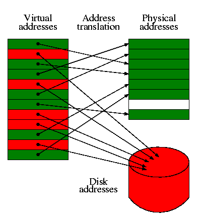
However, the names used are different as illustrated in the table
just below and, as we shall soon see, there are other differences as
well.
| Cache concept | Demand paging analogue |
|---|
| Memory block | Page |
| Cache line | Page Frame (frame) |
| Block Size | Page Size |
| Tag | None (table lookup) |
| Word in block | Page offset |
| Valid bit | Valid bit |
| Miss | Page fault |
| Hit | Not a page fault |
| Miss rate | Page fault rate |
| Hit rate | 1 - Page fault rate |
| Placement question | Placement question |
| Replacement question | Replacement question |
| Associativity | None (fully associative) |
We also need to study the interactions that occur when both caching
and demand paging are employed for the same memory reference.
For both caching and demand paging, the placement
question does not have serious performance implications since the
items are fixed size (no first-fit, best-fit, buddy, etc) as are the
slots into which they are placed.
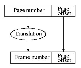
The replacement question, in contrast, is quite
important for performance.
Indeed, we spend significant time discussing replacements strategies
in 202.
Since the immediate past is a reasonably good predictor of the
near-term future, approximations to LRU (least recently used) are
popular for both caching and demand paging.
However, cache approximations are very crude since miss processing
must be very fast and cannot involve a long calculation.
The cost of a page fault vastly exceeds the cost of a cache miss
so it is worth while in paging to slow down hit processing to
lower the miss rate.
Hence demand paging is fully associative and uses a table to
locate the frame in which the page is located.
The two figures on the right and indicate the translation of page
numbers into frame numbers.
The top figure is abstract, the second shows the table actually used
by demand paging for the translation.
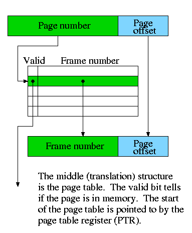
Although both figures are worded in terms of demand paging they can
be interpreted for caching as well by essentially changing the names
of certain concepts and realizing that demand paging corresponds to
the extreme of a fully-associative cache.
- The page number in the diagram becomes the memory block number
when we are discussing caching.
- The page offset becomes the word-in-block.
- Since demand paging uses full associativity, the cache analogue
would have only one set.
Thus the cache index would be zero bits and the tag would be the
entire memory block number (page number in paging).
- The frame number analogue in caching is the cache line
containing the memory block.
The difference in appearance between the bottom diagram and the
various detailed cache diagrams above we have seen previously is
that, unlike a fully associative cache, which would check every cache
block to see if the tags match, demand paging utilizes a (page)
table.
The table approach is simpler as it does not need multiple
comparators; however it is too slow for caches.
What about Writes? (Write Through vs. Write Back)
In this section, read the first element of each parenthesized
pair for caching, and read the second for demand paging.
Question (worded for caches): On a write hit
should we write the new value through to memory or just keep it in
the cache and write it back to memory when the cache-line is
replaced?
Question (worded for demand paging): On a write to
an in-memory page should we write the new value through to disk or
just keep it in the frame and write it back to disk when the page
is replaced?
Answer: It's complicated :-)
- Write through is simpler since write back can require two operations
during a single event (writing back the old line/page and fetching
the new).
- For caching the cost of writing through to memory is around 100
cycles so with a write buffer the cost of write through is
bearable and it does simplify the situation.
Hence writing through is sometimes used, but always with a write
buffer.
- For paging the cost of writing through to disk is on the order
of 1,000,000 cycles.
Since write-back has fewer writes (since multiple writes to the
(cache-line/page) may occur before the (cache-line/page) is
evicted), it is always used for paging.
Making Address Translation Fast: the TLB
A TLB or Translation Lookaside Buffer is a cache of the page table.
It is there for the same reason as any cache, the page table is too
big to access fast enough so we maintain a subset that can be
accessed quickly and (we hope) has few misses.
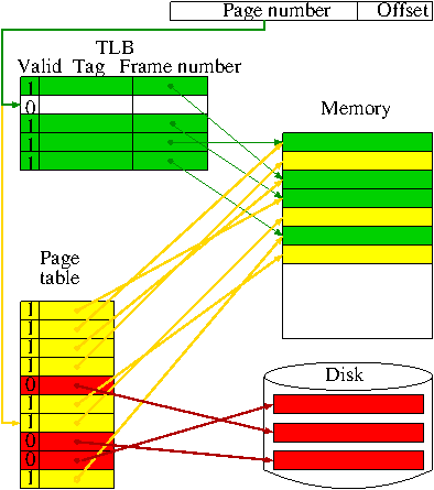
Without a TLB, every memory reference in the program would require
two memory references, one to read the page table and one to read
the requested memory word.
This would be an unacceptable performance loss and hence a TLB is
crucial for a system with paging.
For now, we ignore caching and just look at the TLB, pages, frames,
and the page table.
The diagram on the right shows the three possibilities, color-coded
to indicate their relative speeds.
- Green indicates the fastest path, a TLB hit.
- Yellow indicates the middle speed path, a TLB miss, followed by
a page hit.
- Red indicates the slowest path, a page fault.
- The reference shown quickly checks the TLB and misses.
Then at medium speed it checks the page table and hits.
- Really the page table doesn't point to the disk
block for an invalid entry, but the effect is the same.
Typical TLB parameter values
- Size: hundreds of entries.
- Block size: 1 entry.
- Hit time: 1 cycle.
- Miss time: tens of cycles.
- Miss rate: Low (<= 2%).
Integrating Virtual Memory (Demand Paging), TLBs, and Caches
Real systems have TLBs, page tables, and caches.
Since we shall assume the caches are based on real (not virtual)
memory addresses, the cache can be accessed only after the TLB or
page table has translated the virtual address (page number + offset)
to the real address (frame number + offset).
In some systems, caches are accessed by virtual
address (page number + offset), but we will ignore this
possibility.
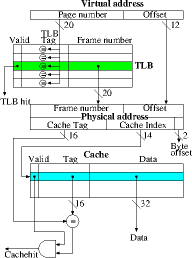
The diagram on the right is based on the decstation 3100, which is
perhaps the simplest possible design.
Recall that the 3100 had the following parameter values.
- Virtual address = 32 bits.
- Physical address = 32 bits.
- Fully associative TLB.
- Direct mapped cache.
- Cache block size = one word.
- Pagesize = 4KB = 2^12 bytes.
- Cache size = 16K entries = 64KB.
Actions taken
- The page number is searched in the fully associative TLB
- If a TLB hit occurs, the frame number from the TLB together
with the page offset gives the physical address.
A TLB miss causes an exception to reload the TLB from the page
table, which the figure does not show.
- The physical address is broken into a cache tag and cache
index (plus a two bit byte offset that is not used for word
references).
- If the reference is a write, just do it (i.e., update the cache
and memory) without checking for a cache hit.
This simplification (doing the same action on a hit as on a miss)
is possible because the cache is primitive as we
discussed previously).
- For a read, if the tag located in the cache entry specified by the
index matches the tag in the physical address, the referenced word has
been found in the cache; i.e., we had a read hit.
- For a read miss, the cache entry specified by the index is
fetched from memory, loaded in the cache (replacing whatever was
in that slot, which is always clean due to the write-through
policy of the cache), and returned to the processor to satisfy the
request.
Start Lecture #27
Hit/Miss possibilities
Before accessing the central memory itself a memory reference may
be looked up in the TLB, the page table, and the cache.
Since all three can be hits or misses, 8 outcomes are theoretically
possible, but only 5 are actually possible.
A page table miss, means a page fault.
For simplicity we assume the memory reference is a read
(i.e., lw, not sw).
| TLB | Page
Table | Cache | Remarks |
|---|
| hit | hit | hit |
Possible, but page table not checked on TLB hit, data from cache |
| hit | hit | miss |
Possible, but page table not checked, data from memory also
loaded in cache
|
| hit | miss | hit |
Impossible, TLB references only in-memory pages |
| hit | miss | miss |
Impossible, TLB references only in-memory pages |
| miss | hit | hit |
Possible, TLB entry loaded from page table, data from cache |
| miss | hit | miss |
Possible, TLB entry loaded from page table, data from memory
also loaded in cache
|
| miss | miss | hit |
Impossible, cache is a subset of memory |
| miss | miss | miss |
Possible, page fault brings in page, TLB entry loaded, cache
loaded
|
Implementing Protection with Virtual Memory
Handling TLB Misses and Page Faults
Summary
Disk access are extremely expensive, which dictates many choices
made for demand paging and explains why choices good for caching
(where a miss costs 10s of a nanosecond),
although valid choices for demand paging, are
not good choices for the latter (where the miss penalty is
several milliseconds).
In particular, demand paging implementations make the following
choices.
- The block size (called the page size for paging) is large (about
1000 words) to take advantage of spacial locality and thereby
lower the all-important miss rate.
- Whereas caches have limited associativity (2-way to 8-way are
common choices), demand paging is a fully-associative cache with
thousands (or more) entries.
- Such high associativity can not be implemented efficiently
with thousands of comparators so a page table is
employed.
- The second memory reference a simple table implies would be
too slow so a TLB is needed.
- Since a page fault is so expensive, elaborate
techniques are used to decide which page to evict.
Matching
| 1. L1 cache | a. Not a cache |
| 2. L2 cache | b. A cache for a cache |
| 3. Memory | c. A cache for disks |
| 4. TLB | d. A cache for main memory |
| 5. Page Table | e. A cache for page table entries |
Do the following two problems in class.
- Match the elements on the left column with the phrase in the
right column that best describes it.
- Consider a memory reference that is miss/miss/miss in the table
above.
In what order are the memory elements in the left column
accessed?
5.8: A Common Framework for Memory Hierarchies
Typical Sizes and Costs
These values, from the book, are for 2012.
Perhaps the most interesting are the miss rate and penalty for
demand paging.
| Feature |
Typical values
for L1 caches |
Typical values
for L2 caches |
Typical values
for Main memory |
Typical values
for TLBs |
| Size | 16KB-64KB | 125KKB-2MB |
1GB-1TB | 256B-16KB |
| Block size | 16B-64B | 64-128 |
4KB-64KB | 4B-32B |
| Miss penalty in clocks | 10-25 | 100-1000 |
10M-100M | 10-1000 |
| Miss rate | 2%-5% | 0.1%-2% |
0.00001%-0.0001% | 0.01%-2% |
Question 1: Where Can/Should the Block Be Placed?
This question has two parts.
- In what slot are we able to place the block.
- For a direct mapped cache, there is only one choice.
- For an n-way associative cache, there are n choices.
- For a fully associative cache, any slot is permitted.
- The n-way case includes both the direct mapped and fully
associative cases.
- For a TLB any slot is permitted.
That is, a TLB is a fully associative cache of the page
table.
- For paging any slot (i.e., any frame) is permitted.
That is, paging uses a fully associative mapping (via a page
table).
- For segmentation, any large enough slot
(i.e., region) can be used.
- If several possible slots are available
(i.e., unoccupied), which one should be used?
- I call this question the placement question.
- For caches, TLBs, and paging, which use fixed size
slots, the question is trivial; any available slot is just
fine.
- For segmentation, the question is
interesting and there are several algorithms, e.g., first fit,
best fit, buddy, etc.
Question 2: How Is a Block Found?
| Associativity | Location method | Comparisons Required |
| Direct mapped | Index | 1 |
| Set Associative | Index the set, search among elements |
Degree of associativity |
| Full | Search all entries |
Number of entries |
| Separate lookup table | 0 |
The difference in sizes and costs for demand paging vs. caching,
leads to different algorithms for finding the block.
Demand paging always uses the bottom row with a separate table (page
table) but caching never uses such a table.
- With page faults so expensive, misses must be reduced as much as
possible.
Hence full associativity is used.
- With such a large associativity (fully associative
with many slots), hardware searching would be
prohibitively expensive and software searching too slow.
Hence a page table is used with a TLB acting as a cache of the
table.
- The large block size in paging (called the page size) means
that the extra page table is a small fraction of the space.
Question 3: Which Block Should Be Replaced?
If no possible slots are available, which victim should be
chosen?
I call this the replacement question and is much
studied in demand paging.
- For demand paging, with miss costs so high and associativity so
large, the replacement policy is very important and some approximation
to LRU is used.
- For caching, even the miss time must be small so simple schemes
are used.
For 2-way associativity, LRU is trivial.
For higher associativity (but associativity is never very high)
crude approximations to LRU may be used and sometimes random
replacement is used.
- For direct mapped caches, the question is trivial.
Since the block can only go in one slot, if you need to place the
block and the only possible slot is occupied, the current resident
of that slot must be the victim.
- For every case except direct mapped caches, namely n-way
associative caches (n>1), TLBs, demand paging, and demand
segmentation, the question is interesting and there are several
algorithms, e.g., LRU, Random, Belady min, FIFO, WS-Clock,
etc.
Question 4: What Happens on a Write?
Write-Through
- Data written to both levels of the hierarchy (the cache and main
memory for caching; main memory and disk for demand paging).
- Sometimes used for caching, never used for demand paging.
- Advantages
- Misses are simpler and cheaper (no copy back).
- Easier to implement, especially for block size 1, which we
did in class.
- For block size > 1, a write miss is more complicated since
the rest of the block now is invalid.
Fetch the rest of the block from memory
or mark those parts invalid by employing extra valid
bits.
Write-Back
- Data written only to the higher (faster but smaller) level of
the hierarchy.
The lower level now has stale data, but becomes up to date when
the block block is subsequently replaced in the higher level.
- Advantages
- Words can be written at the speed of the faster level.
- When block size > 1, writes to multiple words in the cache
block are only written once to memory (when the block is
replaced).
- Multiple writes to the same word in a short
period are written to memory only once.
- When block size > 1, the replacement can utilize a high
bandwidth transfer.
That is, writing one 64-byte block is faster than 16 writes of
4-bytes each.
- Write-back is the only real choice for demand paging since
writing to the lower level of the hierarchy (in this case disk) is
so slow and the block size is so large.
Write Miss Policy
- For demand paging, the case is pretty clear.
Every implementation I know of allocates a frame for the page
miss and fetches the page from disk.
That is it does both an allocate and a
fetch.
- For caching this is not always the case.
Since there are two optional actions there are four
possibilities.
- Don't allocate and don't fetch: This is sometimes called
write around.
It is done when the data is not expected to be read before
it will be evicted.
For example, if you are writing a matrix whose size is much
larger than the cache.
- Don't allocate but do fetch: Impossible, where would you
put the fetched block?
- Do allocate, but don't fetch: Sometimes called
no-fetch-on-write.
Also called SANF (store-allocate-no-fetch).
Requires multiple valid bits per block since the
just-written word is valid but the others are not (since we
updated the tag to correspond to the just-written word).
- Do allocate and do fetch: The normal case we have been
using.
The Three Cs: An Intuitive Model for Understanding the Behavior
of Memory Hierarchies
Compulsory (a.k.a. Cold Start) Misses
Capacity Misses
Conflict Misses
5.9 Using a Finite-State machine to Control a Simple Cache
5.10 Parallelism and Memory Hierarchy: Cache Coherence
5.11 Parallelism and Memory Hierarchy: Redundant Arrays of
Inexpensive Disks
The acronym RAID was coined by Patterson and his students to
abbreviate Redundant Array of Inexpensive Disks.
Now it is often redefined as Redundant Array of Independent Disks.
RAID comes in several flavors often called levels.
Level 0: Striping a.k.a. Interleaving
To increase performance, rather than reliability
and availability, it is a good idea to stripe or interleave blocks
across several disks.
In this scheme block n is stored on disk n mod k, where k is the
number of disks.
The quotient n/k is called the stripe number.
For example, if there are 4 disks, stripe number 0 (the first
stripe) consists of block 0, which is stored on disk 0, block 1
stored on 1, block 2 stored on 2, and block 3 stored on 3.
Stripe 1 (like all stripes in this example) also contains 4 blocks.
The first one is block 4, which is stored on disk 0.
Striping is especially good if one is accessing full stripes in
which case all the blocks in the stripe can be read or written
concurrently.
Since RAID 0 has no redundancy, it offers no reliability advantage.
It does permit large (multi-block) I/Os to use multiple disks and
hence to finish faster.
Level 1: Mirroring
Two disks containing the same content.
- You read from either; in particular concurrent reads of
different blocks are possible.
- A block write is performed on both disks, possibly
concurrently.
- The storage overhead is 100%, i.e. the required storage is
doubled.
- If you are striping across P disks, the mirrored system would
have 2P disks.
Level 2: Error Detecting and Correcting Code
Often called ECC (error correcting code or error
checking and correcting code).
Widely used in RAM, not used as often in for disks.
Level 3: Bit-Interleaved Parity
Normally byte-interleaved or several-byte-interleaved.
For most applications, RAID 4 is better.
Level 4: Block-Interleaved Parity
RAID 4 combines striping and parity.
In addition to the k so-called data disks used in striping, one has
a single parity disk that contains the parity of the stripe.
Consider all k data blocks in one stripe.
Extend this stripe to k+1 blocks by including the corresponding
block on the parity disk.
The block on the parity disk is calculated as the bitwise exclusive
OR of the k data blocks.
Thus a stripe contains k data blocks and one parity block, which is
the exclusive OR of the data blocks.
The great news is that any block in the stripe,
parity or data, is the exclusive OR of the other k.
This means we can survive the failure of any one disk.
For example, let k=4 and let the data blocks be A, B, C, and D.
- If the parity disk fails, we can easily recreate it since, by
definition, the parity block for this stripe is
A ⊕ B ⊕ C ⊕ D
which is the exclusive OR of the other blocks.
- If a data disk fails, we can again recreate it since, by the
properties of XOR,
A ⊕ B ⊕ C ⊕ parity block =
A ⊕ B ⊕ C ⊕ (A ⊕ B ⊕ C ⊕ D)
=
A ⊕ A ⊕ B ⊕ B ⊕ C ⊕ C ⊕
= id ⊕ id ⊕ id ⊕ D = D
and again the missing block is the exclusive OR of the remaining
blocks.
Properties of RAID 4.
- The storage overhead is 1/k.
- ONE failure can be tolerated.
- Failure means detectable failure (disks are good at this).
- A bad disk can be recreated from the remaining disks (and
RAID controllers do this on line).
- In normal operation (i.e., all disks good), reads are not
affected by the redundancy.
In this respect RAID 4 is just like striping.
- When writing a full stripe, the system
calculates the new parity block from the new data blocks and
writes the entire stripe.
- When writing a single block, RAID 4 performs
poorly since it must read additional blocks to determine the new
parity.
- One way would be to read the remaining k-1 data blocks
and calculate the parity as usual.
- There is a better (slightly clever) way.
- If block A is to be changed to A', just read (the old) A
and the old parity P.
The new parity is
A ⊕ A' ⊕ P
- All writes require reading and writing the parity disk, which
becomes a bottleneck and motivates ...
Level 5: Distributed Block-Interleaved Parity
Rotate the disk used for parity.
Again using our 4 data-disk example, we continue to put the parity
for blocks 0-3 on disk 4 (the fifth disk) but
rotate the assignment of which disk holds the parity block of
different stripes.
In more detail.
- For the first stripe block 0 is on 0, 1 is on 1, 2 is on 2, 3
is on 3, and parity is on 4.
- For the next stripe (data blocks 4-7), we put the parity on the
fourth disk so block 4 is on disk 0, 5 is on 1,
6 is on 2, parity is on 3, and 7 is on 4.
- For the next stripe, we put the parity on
the third disk so 8 is on 0, 9 is on 1, parity
is on 2, 10 is on 3, and 11 is on 4.
- etc
Raid 0, Raid 1, and Raid 5 are widely used.
Level 6: P + Q Redundancy
Gives more than single error correction at a higher storage
overhead.
Start Lecture #28
Review (especially lab 7 and practice final)
5.12 Advanced Material; Implementing Cache Controllers
5.13 Real Stuff: The ARM Cortex-A8 and Intel Core i7 Memory
Hierarchies
5.14 Going Faster: Cache Blocking and Matrix Multiply
5.15 Fallacies and Pitfalls
5.16 Concluding Remarks
5.17 Historical Perspective and Further Reading
Chapter 6: Parallel Processors from Client to Cloud
New chapter in 5e
Chapter 6: Storage and Other I/O Topics.
This chapter has been removed in 5e
6.1 Introduction
Peripherals are varied; indeed they vary widely in many dimensions,
e.g., cost, physical size, purpose, capacity, transfer rate,
response time, support for random
access, connectors, and
protocol.
Consider just transfer rate for the moment.
- Some devices like keyboards and mice have tiny data rates.
- Printers, etc have moderate data rates.
- Disks and fast networks have high data rates.
- A good graphics card and monitor has a huge data rate.
The text mentions three especially important characteristics which
can be used to classify peripherals.
- Input vs. output vs. storage.
A keyboard is an input device (meaning the device produces data
that is input by the processor).
A printer is an output device (meaning ...).
A disk is a storage device (meaning it can be read, reread,
written, and rewritten.
- Used directly by a human (e.g. a monitor).
- Data rate (i.e., transfer rate).
Performance Metrics
Probably the most important quality metric for I/O is not
performance but how frequently is data irretrievably corrupted.
We will soon discuss RAID, a technique to improve this metirc.
There are at least three ways to measure I/O performance
- How much data can be processed per second.
This metric normally improves as the size of each request
increases since there is normally a
startup overhead
for
each request.
- How many operations can be performed per second.
This metric normally degrades as the size of each request
increases.
- How long does a single request take.
This metric normally degrades as the size of each request
increases.
Do not make the error of thinking that the 3rd metric is simply
the reciprocal of the second.
It takes the post office at least one day to deliver a letter from
here to California, but I can send one every minute if I wish.
This is another example of pipelining.
6.2 Dependability, Reliability, and Availability
A system alternates between two states of delivered service
- The service is delivered as specified.
- The service is not delivered as specified.
Transitioning from the first state to the second is called a
failure.
Transitioning from the second state to the first is called a
restoration.
Reliability measures the length of time during
which services is continuously delivered as expected.
An example reliability measure is
mean time to failure (MTTF), which measures the
average length of time that the system is delivering service as
expected.
Bigger values are better.
Another important measure is
mean time to repair (MTTR), which measures how
long the system is not delivering service as expected.
Smaller values are better.
Finally we have mean time between failures
(MTBF).
MTBF = MTTF + MTTR.
One might think that having a large MTBF is good, but that
is not necessarily correct.
Consider a system with a certain MTBF and simply have the repair
center deliberately add an extra 1 hour to the repair time and poof
the MTBF goes up by one hour!
6.3 Disk Storage
Devices are quite varied and their data rates vary enormously.
Show a real disk opened up and illustrate the components.
- Platter
- Surface
- Head
- Track
- Sector
- Cylinder
- Seek time
- Rotational latency
- Transfer time
Disk Access Time
The time for a disk access has five components, of which we
concentrate on the first three.
- Seek.
- Rotational latency.
- Transfer time.
- Controller overhead.
- Queuing delays.
Seek Time
Today seek times are typically 3-8ms
on average
.
It takes longer to go all the way across the disk but it
does not take twice as long to go twice as far (the
head must accelerate, decelerate, and settle on the track).
How should we calculate the average?
- Add the times for all possible seeks and divide by the number
of possible seeks (of course!).
- But systems achieve average seek times much
smaller than this.
How?
- Locality of reference!
So most seeks are small.
The locality is further enhanced by disk scheduling algorithms.
- Caches (again)!
Disks have (electronic, not mechanical) caches.
Rotational Latency
Since disks have just one arm the average
rotational latency is half the time of a revolution, and is thus
determined by the RPM (revolutions per minute) of the disk.
Disks today spin at 5400-15,000 RPM; they used to all spin at 3600
RPM.
Calculate on the board the average rotational latency of a 3600 RPM
disk.
Homework:
What is the average rotational latency for a 5400 RPM disk, a 5400
RPM disk, a 10,000 RPM, and a 15,000 RPM disk.
Transfer Time
You might consider the other four times all overhead
since it is the transfer time during which the data is actually
being supplied.
The transfer rate is typically tens of MB
per second, sometimes over 100MB/sec.
Given the rate, which is determined by the disk in use, the transfer
time is proportional to the length of the request.
Some manufacturers quote a much higher rate, but that is for cache
hits.
In addition to supplying data much sooner, the electronic cache can
transfer data at a higher rate than the mechanical disk.
Consider a disk with a 5ns seek time, a transfer rate of 80MB/sec,
and a rotational rate of 10,000 RPM.
Calculate on the board how long it takes for a 1K block request to
What overall transfer rate (bytes delivered / total time) was
achieved.
Homework:
Consider a disk with a 6ns seek time, a transfer rate of 60MB/sec,
and a rotational rate of 10,000 RPM.
How long does a request for a 100K block require to complete?
A 10MB block?
What overall transfer rates (bytes delivered / total time) were
achieved in each case.
Controler Time
Not much to say.
It is typically small.
We will use 0ms (i.e., ignore this time).
Queuing Delays
This can be the largest component, but we will
ignore it since it is not a function of the architecture, but rather
of the load and OS.
6.4 Flash Storage
Often called a solid-state disk, flash is the latest attempted
gap-filler
technology, i.e., a technology between
RAM
and conventional disks.
Unlike most past efforts, this one has succeeded to some extent.
Flash is between DRAM and disks in both price and performance: it
is cheaper and slower than DRAM, but more expensive and faster than
disks.
However, the minimal size disk is much larger than the minimal size
flash and hence, for devices with a modest memory requirement, flash
is cheaper than (as well as faster than) a disk.
Other advantages of flash over disks include lower power, smaller
physical size, silence, and shock resistance.
These are due to the semiconductor nature of flash implying that it
has no moving parts.
Technically flash is a kind of EEPROM, an electrically erasable,
programmable read-only memory.
Like other EEPROM technologies, but unlike DRAM, flash retains the
values stored when power is turned off, a crucial requirement for a
disk replacement.
Another typical characteristic of EEPROMs shared by flash is a
significantly limited lifetime with respect to writing.
A given flash cell can be rewritten many thousands of times, but not
millions of times.
This is a serious limitation and solid state disks contain software
that remap heavily used flash blocks to other flash cells, a
technique called wear leveling.
There are two flavors of flash called NOR and NAND.
The former is older technology, but has higher performance primarily
because NAND can be read and written only in large blocks.
NAND flash is increasingly popular due to is lower price ($4/GB in
2008, compared to $65/GB for NOR).
Today (Dec, 2011) NAND is available for about $1/GB about 10 times
the price per byte of a very large disk.
6.5: Connecting Processors, Memory, and I/O Devices
A bus is a shared communication link, using one set of wires to
connect many subsystems.
- Sounds simple (once you have tri-state drivers) ...
- ... but it's not.
- There are very serious electrical considerations (e.g. signals
reflecting from the end of the bus).
We have ignored (and will continue to ignore) all electrical
issues.
- Getting high speed buses is state-of-the-art engineering.
Tri-state Drivers
- A output device that can either
- Drive the line to 1.
- Drive the line to 0.
- Not drive the line at all (be in a high impedance state).
- It is possible have many of these devices devices connected to
the same wire providing you are careful to be sure that all but
one are in the high-impedance mode.
- This is why a single bus can have many output devices attached
(but only one actually performing output at a given time).
Bus Basics
- Buses support bidirectional transfer, sometimes using separate
wires for each direction, sometimes not.
- Normally the processor-memory bus (a.k.a memory bus) is kept
separate from the I/O bus.
It is a fast synchronous bus (see next section)
and I/O devices can't keep up.
- Indeed the memory bus is normally custom designed (i.e., companies
design their own).
- The graphics bus is also kept separate in modern designs for
bandwidth reasons, but often is an industry standard (e.g. the AGP
bus).
- Many I/O buses are industry standards (ISA, EISA, SCSI, PCI) and
support open architectures, where components can
be purchased from a variety of vendors.
- The processor memory bus has the highest bandwidth, the
backplane bus less and the I/O buses the least.
Clearly the (sustained) bandwidth of each I/O bus is limited by
the backplane bus.
Why?
Answer: Because all the data passing on an I/O bus must also pass
on the backplane bus.
- Bus adaptors are used as interfaces between buses.
They perform speed matching and may also perform buffering, data
width matching, and converting
between synchronous and
asynchronous buses (see next section).
Synchronous vs. Asynchronous Buses
A synchronous bus is clocked.
- One of the lines in the bus is a clock that serves as the clock
for all the devices on the bus.
- All the bus actions are done on fixed clock cycles.
For example, 4 cycles after receiving a request, the memory
delivers the first word.
- This can be handled by a simple finite state machine (FSM).
Basically, once the request is seen everything works one clock at
a time.
There are no decisions like the ones we will see for an
asynchronous bus.
- Because the protocol is so simple, it requires few gates and is
very fast.
So far so good.
- Two problems with synchronous buses.
- All the devices must run at the same speed.
- The bus must be short due to
clock skew.
- Processor to memory buses are now normally synchronous.
- The number of devices on the bus are small.
- The bus is short.
- The devices (i.e. processor and memory) are prepared to
run at the same speed.
- High speed is crucial.
An asynchronous bus is not
clocked.
- Since the bus is not clocked devices of varying speeds can be on the
same bus.
- There is no problem with clock skew (since
there is no clock).
- But the bus must now contain control lines to coordinate
transmission.
- Common is a handshaking protocol.
Consider the situation pictured at right where a device receives
an I/O request and then needs to retrieve some data from memory.
We are using an asynchronous bus for the memory request and
transfer.
Recall that this means, neither the device nor the memory knows the
speed of its partner and must be prepared for very long or
essentially instantaneous responses.
Note that Ack is bidirectional.
We must insure that both sides are never driving
(outputting
on) this line at the same time.
You may think of Ack as two lines, one going in each
direction
but, in fact, one line is sufficient if tri-state drivers are
used.
A similar consideration applies to the Data Lines.
We describe below the protocol used between the device and the
memory and illustrate on the right a finite state machine used to
manage this interactions.
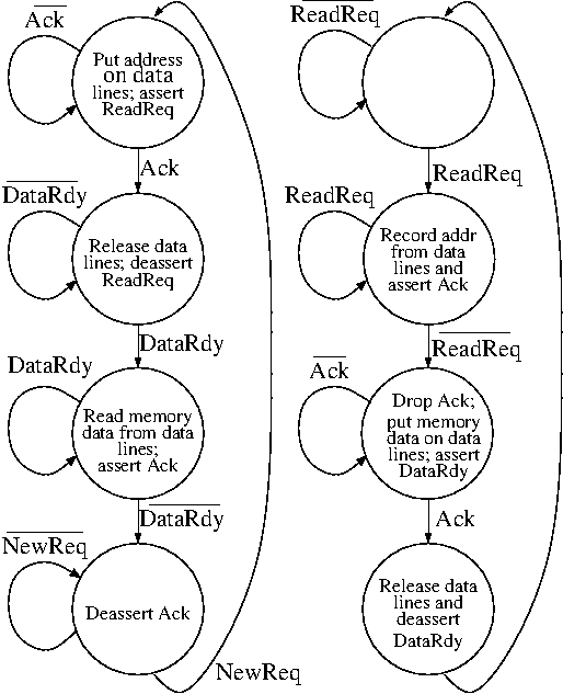
The system is initialized with the memory in the top right state
and the device in the top left state.
Ack is not asserted by either side.
ReadReq, DataRdy, and
NewReq are also
deasserted.
At some point an external entity (likely the CPU)
raises NewReq.
Events then proceed as follows.
- The device makes a request (asserts ReadReq and puts the
desired address on the data lines).
The name data lines sounds odd since it is (now) being used for
the address.
It will also be used for the data itself in this design.
Data lines should be contrasted with control lines (such as
ReadReq).
- Memory, which has been waiting, sees ReadReq, records the
address and asserts Ack.
- The device waits for the Ack; once seen, it drops the
data lines and deasserts ReadReq.
- The memory waits for the request line to drop.
Then it can drop Ack (which it knows the device has now seen).
The memory now at its leasure puts the data on the data lines
(which it knows the device is not driving) and then asserts
DataRdy.
(DataRdy has been deasserted until now).
- The device has been waiting for DataRdy.
It detects DataRdy and records the data.
It then asserts Ack indicating that the data has been read.
- The memory sees Ack and then deasserts DataRdy and releases the
data lines.
- The device seeing DataRdy low deasserts Ack ending the show.
Note that both sides are prepared for another performance.
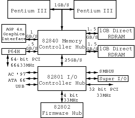
The Buses and Networks of the Pentium III
For a realistic example, on the right is a diagram adapted from
the 25 October 1999 issue of Microprocessor Reports on a
then brand new Intel chip set, the so called 840.
Bus adaptors have a variety of names, e.g. host adapters, hubs,
bridges.
The memory controller hub is often call the north bridge and the I/O
controller hub is often called the south bridge.
Bus lines (i.e., wires) include those for data, function codes,
device addresses.
Data and address are considered data and the function codes are
considered control (remember our datapath for MIPS).
Address and data may be multiplexed on the same lines (i.e., first
send one then the other) or may be given separate lines.
One is cheaper (good) and the other has higher performance (also
good).
Which is which?
Ans: the multiplexed version is cheaper.
Improving Bus Performance
These improvements mostly come at the cost of increased expense and/or
complexity.
- A multiplicity of buses as in the Pentium III diagram above.
- Synchronous instead of asynchronous protocols.
Synchronous is actually simplier, but it essentially implies a
multiplicity of buses, since not all devices can operate at the
same speed.
- Wider data path: Use more wires, send more data at one time.
- Separate address and data lines: Same as above.
- Separate wires for each direction.
- Block transfers: Permit a single transaction to transfer more
than one busload of data.
Saves the time to release and acquire the bus, but the protocol
is more complex.
Obtaining bus access
- The simplest scheme is to permit only one bus
master.
- That is, on each bus only one device is permited to
initiate a bus transaction.
- The other devices are slaves that only
respond to requests.
- With a single master, there is no issue of arbitrating among
multiple requests.
- The example we just did had only one master (all requests
initiated on the left).
- One can have multiple masters with daisy
chaining of the grant line.
- Any device can assert the request line, indicating that it
wishes to use the bus.
- This is not trivial:
uses
open collector drivers
.
- If no output drives the line, it will
be
pulled up
to 5v, i.e., a logical true.
- If one or more outputs drive the line
to 0v it will go to 0v (a logical false).
- So if a device wishes to make a request
it drives the line to 0v; if it does not wish to make a
request it does nothing.
- This is (another example of) active low
logic.
The request line is asserted by driving it low.
- When the arbiter sees the request line asserted (and the
previous grantee has issued a release), the arbiter raises the
grant line.
- Note that the arbiter does not know which
device has made the request; it knows only that a request has
been made.
- The grant signal is passed from one device to another if the
first device is not requesting the bus.
Hence devices near the arbiter have priority and can starve
the ones further away.
- The device whose request is granted asserts the release line
when done.
- Simple, but not fair and not of high performance.
- Centralized parallel arbiter: Separate request lines from each
device and separate grant lines.
The arbiter decides which device should be granted the
bus.
- Distributed arbitration by self-selection: Requesting
processes identify themselves on the bus and decide individually
(and consistently) which one gets the grant.
- Distributed arbitration by collision detection: Each device
transmits whenever it wants, but detects collisions and retries.
The original ethernet uses this scheme (but modern switched
ethernets do not).
Cost Performance Tradeoffs
| Option | High performance | Low cost |
|---|
| bus width | separate addr and data lines |
multiplex addr and data lines |
| data width | wide | narrow |
| transfer size | multiple bus loads |
single bus loads |
| bus masters | multiple | single |
| clocking | synchronous | asynchronous |
Do on the board the following example.
Given
- The memory and bus support two widths of data transfer: 4
words and 16 words.
- The bus is synchronous.
- 200MHz clock.
- 1 clock (this means one cycle) to send address.
- 2 clocks to send data.
- 2 clocks of
rest
between bus accesses.
- Memory access times: 4 words in 200ns; each additional 4 words
in 20ns.
- The system can overlap transferring data with reading more
data.
Find
- Sustained bandwidth and latency for reading 256 words using
4 word transfers.
- Sustained bandwidth and latency for reading 256 words using
16 word transfers.
- How many bus transactions per sec for each (a transaction
includes both address and data.
Solution with four word blocks.
- 1 clock to send addr.
- 40 clocks to read the memory.
- 2 clocks to send data.
- 2 idle clocks.
- 45 total clocks for one transaction.
- 256/4=64 transactions needed so latency is
64*45*5ns=14.4μs.
- Bandwidth = 1024 bytes per 14.4μs = 71.11MB/sec
- 64 transactions per 14.4μs gives 4.44 mega-transactions per
sec.
Solution with sixteen word blocks
- 1 clock for addr.
- 40 clocks for reading first 4 words.
- 2 clocks to send.
- 2 clocks idle.
- 4 clocks to read next 4 words.
But this is free! Why?
Because it is done during the send and idle of previous
block.
- So the only memory access time we wait for is the long initial
read.
- Total = 1 + 40 + 4*(2+2) = 57 clocks.
- 256/16=16 transactions needed so latency is 57*16*5ns=4.5μs.
- This is much better than with 4 word blocks.
- 16 transactions per 4.56μs = 3.51M transactions/sec.
- Bandwidth = 1024B per 4.56μs = 224.56MB/sec.
Homework:
Redo the last example but do not permit
transmitting data to overlap reading more data.
6.6: Interfacing I/O Devices to the Processor, Memory, and Operating
System
This is an I/O issue and is taught in 202.
Giving commands to I/O Devices
This is really an OS issue.
Must write/read to/from device registers, i.e. must communicate
commands to the controller.
Note that a controller normally contains a microprocessor, but
when we say the processor, we mean the central processor not the
one on the controller.
- The controler has a few registers that can be read and/or
written by the processor, similar to how the processor reads
and writes memory.
These registers are also read and written by the controller.
- Nearly every controler contains
- A data register, which is readable (by the processor)
for an input device (e.g., a simple keyboard), writable
for an output device (e.g., a simple printer), and both
readable and writable for input/output devices (e.g.,
disks).
- A control register for giving commands to the device.
- A readable status register for reporting errors and
announcing when the device is ready for the next action
(e.g., for a keyboard telling when the data register is
valid, and for a printer telling when the character to be
printed has be successfully retrieved from the data
register).
Remember the communication protocol we studied where ack
was used.
- Many controllers have more registers
Communicating with the Processor
Should we check periodically or be told when there is something
to do?
Better yet can we get someone else to do it since we are not
needed for the job?
- We get mail at home once a day.
- At some business offices mail arrives a few times per day.
- No problem checking once an hour for mail.
- If email wasn't buffered, you would have to check several
times per minute (second?, millisecond?).
- Checking email this often is too much of a burden and most of the
time when you check you find there is none so the check was wasted.
Polling
Processor continually checks the device status to see if action is
required.
- Like the mail example above.
- For a general purpose OS, one needs a timer to tell the
processor it is time to check (OS issue).
- For an embedded system (microwave) make the checking part of
the main control loop, which is guaranteed to be executed at a
minimum frequency (application software issue).
- For a keyboard or mouse, which have very low data rates, the
system can afford to have the main CPU check.
We do an example just below.
- It is a little better for slave-like output devices such as
a simple printer.
Then the processor only has to poll after a request has been
made until the request has been satisfied.
Do on the board the example on pages 676-677
- Cost of a poll is 400 clocks.
- CPU is 500MHz.
- How much of the CPU is needed to poll
- A mouse that requires 30 polls per sec?
- A floppy that sends 2 bytes at a time and achieves
50KB/sec?
- A hard disk that sends 16 bytes at a time and achieves
4MB/sec?
- For the mouse, we use 12,000 clock cycles each second sec for
polling.
The CPU runs at 500*106 cycles/sec.
So polling the mouse requires 12/500*10-3 =
2.4*10-5 of the CPU.
A very small penalty.
- The floppy delivers 25,000 (two byte) data packets per second
so we must poll at that rate not to miss one.
CPU cycles needed each second is (400)(25,000)=107.
This represents 107 / 500*106 = 2% of the
CPU.
- To keep up with the disk requires 250K polls/sec or
108 clock cycles or 20% of the CPU.
- The system need not poll the floppy and disk until the CPU had
issues a request.
But then it must keep polling until the request is satisfied.
Interrupt driven I/O
Processor is told by the device when to look.
The processor is interrupted by the device.
- Dedicated lines (i.e. wires) on the bus are assigned for
interrupts.
- When a device wants to send an interrupt it asserts the
corresponding line.
- The processor checks for interrupts after each instruction.
This requires
zero time
as it is done in parallel with
the instruction execution.
- If an interrupt is pending (i.e., if a line is asserted) the
processor (this is mostly an OS issue, covered in 202).
- Saves the PC and perhaps some registers.
- Switches to kernel (i.e., privileged) mode.
- Jumps to a location specified in the hardware (the
interrupt handler).
At this point the OS takes over.
- What if we have several different devices and want to do
different things depending on what caused the interrupt?
- Use vectored interrupts.
- Instead of jumping to a single fixed location, the
system defines a set of locations.
- The system might have several interrupt lines.
If line 1 is asserted, jump to location 100, if line 2 is
aserted jump to location 200, etc.
- Alternatively, the system could have just one line and
have the device send the addressto jump to.
- There are other issues with interrupts that are taught in
OS.
For example, what happens if an interrupt occurs while an
interrupt is being processed.
For another example, what if one interrupt is more important
than another.
These are OS issues and are not covered in this course.
- The time for processing an interrupt is typically longer
than the type for a poll.
But interrupts are not generated when the device is
idle, a big advantage.
Do on the board the example on pages 681-682.
- Same hard disk and processor as above.
- Cost of servicing an interrrupt is 500 cycles.
- The disk is active only 5% of the time.
- What percent of the processor would be used to service the
interrupts?
- Cycles/sec needed for processing interrupts while the disk
is active is 125 million.
- This represents 25% of the processor cycles available.
- But the true cost is only 1.25%, since the disk is active
only 5% of the time.
- Note that the disk is not active (i.e., actively generating
interrupts) right after the request is made.
Interrupts are not generated during the seek and rotational
latency.
They are generated only during the transfer itself.
Direct Memory Access (DMA)
The processor initiates the I/O operation then something
else
takes care of it and notifies the processor when it is
done (or if an error occurs).
- Have a DMA engine (a small processor) on the controller.
- The processor initiates the DMA by writing the command into
data registers on the controller (e.g., read sector 5, head 4,
cylinder 123 into memory location 34500).
- For commands that are longer than the size of the data
register(s), a protocol must be used to transmit the
information.
- (I/O done by the processor as in the previous methods is
called programmed I/O, PIO).
- The controller collects data from the device and then sends
it on the bus to the memory without bothering the CPU.
- So we have a multimaster bus and need some sort of
arbitration.
- Normally the I/O devices are given higher priority than
the CPU.
- Freeing the CPU from this task is good but isn't as
wonderful as it seems since the memory is busy (but cache
hits can be processed).
- A big gain is that only one bus transaction is needed
per bus load.
With PIO, two transactions are needed: controller to
processor and then processor to memory.
- This was for an input operation (the controller writes
to memory).
A similar situation occurs for output where the controller
reads from the memory).
Once again one bus transaction per bus load.
- When the controller detects that the I/O is complete or if
an error occurs, it sets the status register accordingly and
sends an interrupt to the processor to notify the latter that
the I/O is complete.
More Sophisticated Controllers
- Sometimes called
intelligent
device controlers, but I
prefer not to use anthropomorphic terminology.
- Some devices, for example a modem on a serial line, deliver
data without being requested to.
So a controller may need to be prepared for unrequested
data.
- Some devices, for example an ethernet, have a complicated
protocol so it is desirable for the controller to process some
of that protocol.
In particular, the collision detection and retry with
exponential backoff characteristic of (non-switched) ethernet
requires areal program.
- Hence some controllers have microprocessors on board that
handle much more than block transfers.
- In the old days there were I/O channels, which would execute
programs written dynamically by the main processor.
For the modern controllers, the programs are fixed and loaded in
ROM or PROM.
Subtleties involving the memory system
- Having the controller simply write to memory doesn't update
the cache.
Must at least invalidate the cache line.
- Having the controller simply read from memory gets old values
with a write-back cache.
Must force write backs.
- The memory area to be read or written is specified by the
program using virtual addresses.
But the I/O must actually go to physical addresses.
Need helpfrom the MMU.
6.7 I/O Performace Measures: Examples from Disk and File Systems
Transaction Processing I/O Benchmarks
File System and Web I/O Benchmarks
I/O Performance versus Processor Performance
We do an example to illustrate the increasing impact of I/O
time.
Assume
- A job currently takes 100 seconds of CPU time and 50 seconds
of I/O time.
- The CPU and I/O times can not be overlapped.
Thus the total time required is 150 seconds.
- The CPU speed increases at a rate of 40% per year.
This implies that the CPU time required in year n+1 is (1/1.4)
times the CPU time required in year n.
- The I/O speed increases at a rate of 10% per year.
Calculate
- The CPU, I/O, and overall time required after 1,2,5,10,20 years.
- The percentage of the job time that the CPU is active for each
year.
- The CPU, I/O, and overall speedup for each year.
Homework: Redo the
above example assuming that CPU and I/O activity can be overlapped,
i.e., assume the overall time is MAX(CPU,I/O) rather than
SUM(CPU,I/O)?
6.8: Designing an I/O system
Recall the picture on the right.
When we are dealing with disks, the bus adapters between the
backplane bus and the various I/O buses are called disk
controllers.
On each of those I/O buses, one would find disks.
Assume a system with the following characteristics is executing a
workload of 64KB reads with 100K instructions between reads..
- A CPU that executes 300 million instructions/sec.
- 50K (OS) instructions required for each I/O.
- A Backplane bus (on which all I/O travels) that supports a
data rate of 100MB/sec.
- Disk controllers supporting a data rate of 20MB/sec and
accommodating up to 7 disks.
- Disks with bandwidth 5MB/sec and seek plus rotational latency
of 10ms.
Find
- The maximum I/O rate achievable.
- How many controllers are needed for this rate?
- How many disks are needed for this rate?
Solution
- One I/O plus the user's code between I/Os takes 150,000
instructions combined.
- So the CPU limits us to 2000 I/O per sec.
- The backplane bus limits us to 100 million / 64,000 = 1562 I/Os
per sec.
- Hence the CPU limit is not relevant and the maximum I/O rate is
1562 I/Os per sec.
- The disk time for each I/O is 10ms + (64KB / (5MB/sec)).
= 10ms + (12.8*10-3)sec = 22.8ms.
- So each disk can achieve 1/(.0228) = 43.9 I/Os per sec.
- So need ⌈1562/43.9⌉ = 36 disks.
- Each disk uses 64KB/22.8ms = 2.74 MB/sec of bus bandwidth.
- Since the controller supports 20 MB/sec, we can put 7 disks (the
maximum permitted) on it without it saturating.
- So, to support 36 disks we need 6 controllers (not all will
have 7 disks).
Remark: The above analysis was very simplistic.
It assumed everything overlapped just right and the I/Os were not
bursty and that the I/Os conveniently spread themselves accross the
disks.
Homework:
Redo the above with the following parameters (more reflective of
2011 technology).
Parameters not mentioned should be given the values in the example
and your work should make the same simplistic assumptions that were
made in the analysis.
- The CPU executes 2 billion instructions/sec.
- The backplane bus bandwidth is 8GB/sec.
- A disk controller supports up to 15 disks and has a total
bandwidth of 1GB/sec.
- Disks have bandwidth 50MB/sec and a seek plus rotational delay
of 8ms.
6.9 Parallelism and I/O: Redundant Arrays of Inexpensive Disks (RAID)
Moved to 5.11 in 5e
6.10 Real Stuff: Sun Fire x4150 Server
6.11 Advanced Topics: Networks
6.12 Fallacies and Pitfalls
6.13 Concluding Remarks
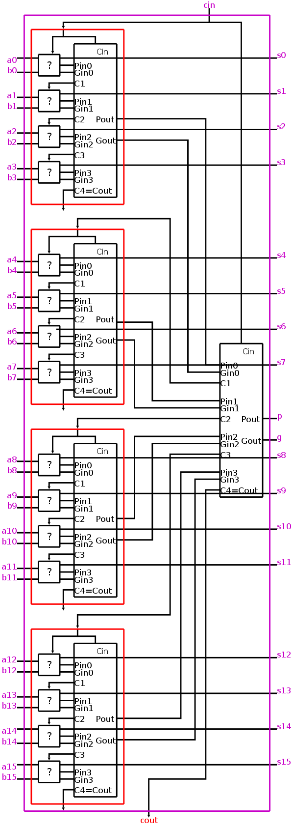