Computer Architecture
Start Lecture #17
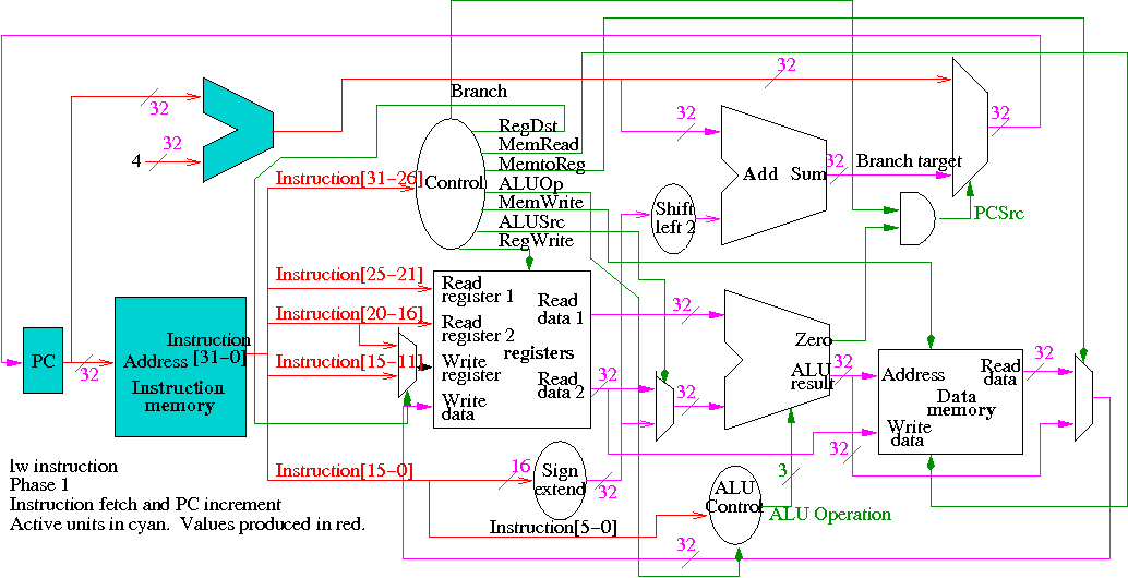
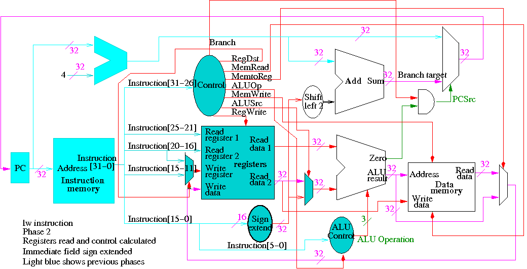
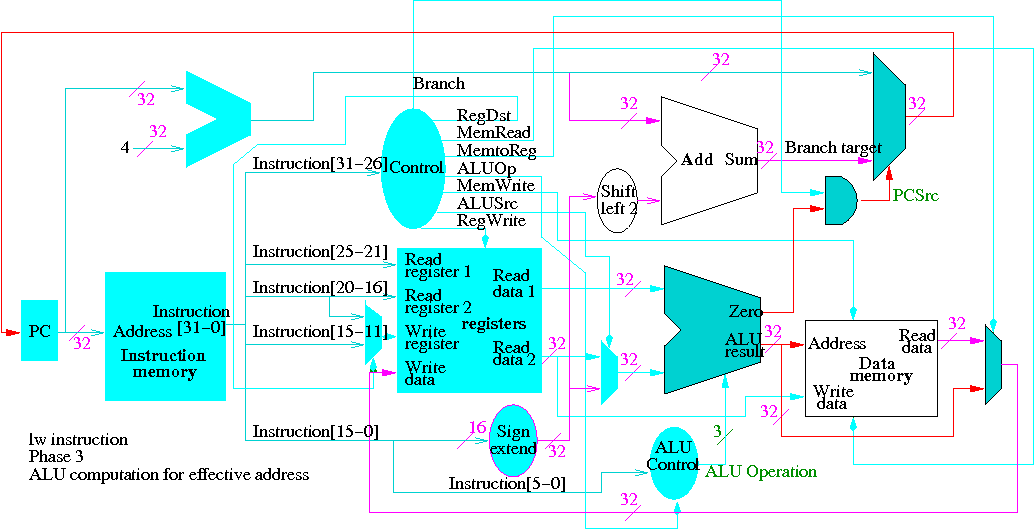
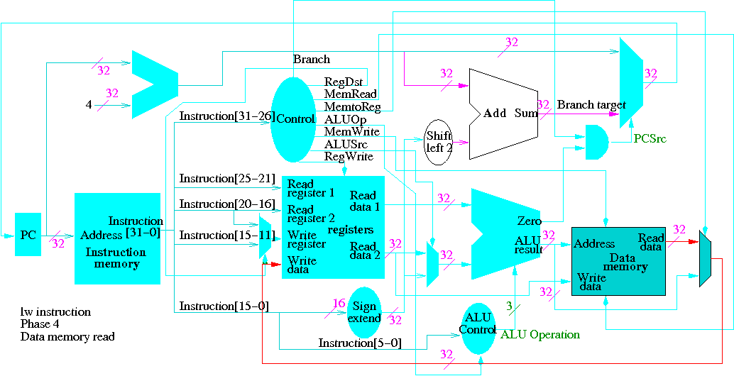
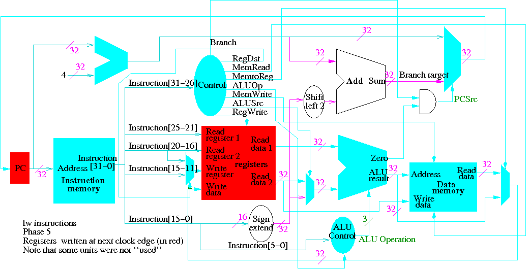
Next we show lw
The following truth table shows the settings for the control lines
for each opcode.
This is drawn differently since the labels of what should be the
columns are long (e.g. RegWrite) and it is easier to have long
labels for rows.
| Signal | R-type | lw | sw | beq |
|---|
| Op5 | 0 | 1 | 1 | 0 |
| Op4 | 0 | 0 | 0 | 0 |
| Op3 | 0 | 0 | 1 | 0 |
| Op2 | 0 | 0 | 0 | 1 |
| Op1 | 0 | 1 | 1 | 0 |
| Op0 | 0 | 1 | 1 | 0 |
|
|
|
|
|
| RegDst | 1 | 0 | X | X |
| ALUSrc | 0 | 1 | 1 | 0 |
| MemtoReg | 0 | 1 | X | X |
| RegWrite | 1 | 1 | 0 | 0 |
| MemRead | 0 | 1 | 0 | 0 |
| MemWrite | 0 | 0 | 1 | 0 |
| Branch | 0 | 0 | 0 | 1 |
| ALUOp1 | 1 | 0 | 0 | 0 |
| ALUOp0 | 0 | 0 | 0 | 1 |
If drawn the normal way the table would look like this.
| Op5 | Op4 | Op3 | Op2 | Op1 | Op0
| RegDst | ALUSrc | MemtoReg | RegWrite | MemRead | MemWrite
| Branch | ALUOp1 | ALUOp0 |
|---|
|
|
|---|
| 0 | 0 | 0 | 0 | 0 | 0
| 1 | 0 | 0 | 1 | 0 | 0 | 0 | 1 | 0 |
|---|
| 1 | 0 | 0 | 0 | 1 | 1
| 0 | 1 | 1 | 1 | 1 | 0 | 0 | 0 | 0 |
|---|
| 1 | 0 | 1 | 0 | 1 | 1
| X | 1 | X | 0 | 0 | 1 | 0 | 0 | 0 |
|---|
| 0 | 0 | 0 | 1 | 0 | 0
| X | 0 | X | 0 | 0 | 0 | 1 | 0 | 1 |
|---|
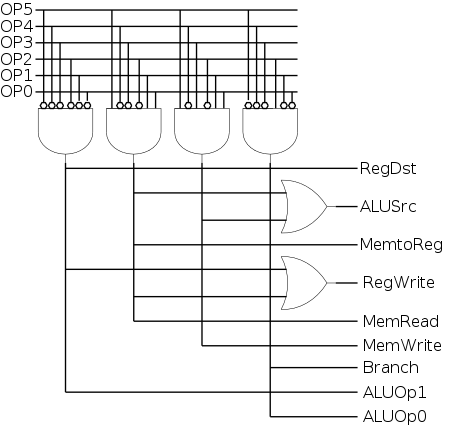
Now it is straightforward to get the logic equations.
The circuit, drawn in PLA style (2-levels of logic) is shown on the
right.
Homework:
In a previous homework, you modified the datapath to support addi and
a variant of lw.
Determine the control needed for these instructions.
5.15, 5.16
Homework (part of 5.13):
Can we eliminate MemtoReg and use MemRead instead?
Homework:
Can any other control signals be eliminated?
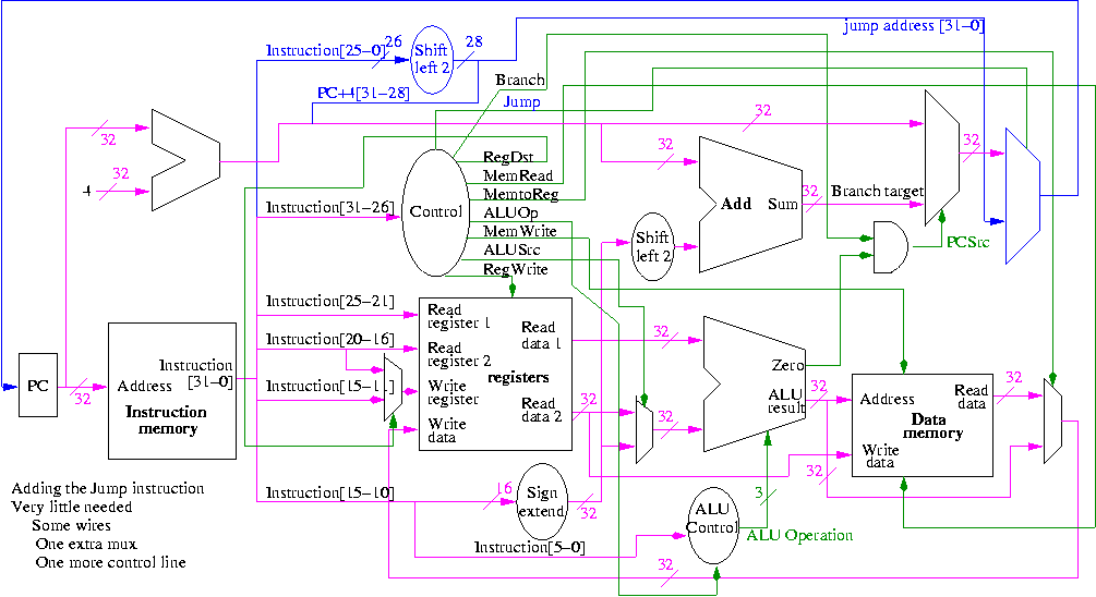
Implementing a J-type instruction, unconditional jump
Recall the jump instruction.
    opcode  addr
    31-26   25-0
Addr is a word address; the bottom 2 bits of the PC are always 0;
and the top 4 bits of the PC are unchanged (AFTER incrementing by 4).
This is quite easy to add and smells like a good final exam question.
What's Wrong
Some instructions are likely slower than others and we must set the
clock cycle time long enough for the slowest. The disparity between
the cycle times needed for different instructions is quite significant
when one considers implementing more difficult instructions, like
divide and floating point ops. Actually, if we considered cache
misses, which result in references to external DRAM, the cycle time
ratios exceed 100.
Possible solutions
- Variable length cycle. How do we do it?
- Asynchronous logic
Self-timed
logic.
- No clock.
Instead each signal (or group of signals) is
coupled with another signal that changes only when the first
signal (or group) is stable.
- Hard to debug.
-
Multicycle instructions.
- More complicated instructions have more cycles.
- Since only one instruction is executed at a time, can reuse a
single ALU and other resourses during different cycles.
- It is in the book right at this point but we are not
covering it now; perhaps later.
Even Faster (we are not covering this).
- Pipeline the cycles.
- Since at one time we will have several instructions active, each
at a different cycle, the resources can't be reused (e.g., more
than one instruction might need to do a register read/write at one
time).
- Pipelining is more complicated than the single cycle
implementation we did.
- This was the basic RISC technology on the 1980s.
- A pipelined implementation of the MIPS CPU is covered in chapter 6.
- Multiple datapaths (superscalar).
- Issue several instructions each cycle and the hardware
figures out dependencies and only executes instructions when the
dependencies are satisfied.
- Much more logic required, but conceptually not too difficult
providing the system executes instructions in order.
- Pretty hairy if out of order (OOO) exectuion is
permitted.
- Current high end processors are all OOO superscalar (and are
indeed pretty hairy).
- A very modern consideration is that performance per
transistor is going down and that it would/might be
better to have many simple processors on a chip rather that
one or a few complicated ones
- VLIW (Very Long Instruction Word)
- User (i.e., the compiler) packs several instructions
into one
superinstruction
called a very long
instruction.
- User guarentees that there are no dependencies within a
superinstruction.
- Hardware still needs multiple datapaths (indeed the
datapaths are
not so different from superscalar).
- The hairy control for superscalar (especially OOO
superscalar) is not needed since the dependency checking
is done by the compiler, not the hardware.
- Was proposed and tried in 80s, but was dominated by
superscalar.
- A comeback (?) with Intel's EPIC (Explicitly Parallel
Instruction Computer) architecture.
- Called IA-64 (Intel Architecture 64-bits); the first
implementation was called Merced and now has a funny name
(Itanium).
It became available in the 1990s
- It has other features as well (e.g. predication).
- The x86, Pentium, etc are called IA-32.
- Has not done well and appears dead/dieing.