Start Lecture #16
How should we implement this?
We will do it PLA style (disjunctive normal form, 2-levels of logic).
When is Bnegate (called Op2 in book) asserted?
Ans: Those rows where its bit is 1, namely rows 2, 4, and 7.
    ALUOp | Funct
    1 0   | 5 4 3 2 1 0
    ------+------------
    x 1   | x x x x x x
    1 x   | x x 0 0 1 0
    1 x   | x x 1 0 1 0
Notice that, in the 5 rows with ALUOp=1x, F1=1 is enough to distinugish the two rows where Bnegate is asserted. This gives
    ALUOp | Funct
    1 0   | 5 4 3 2 1 0
    ------+-------------
    x 1   | x x x x x x
    1 x   | x x x x 1 x
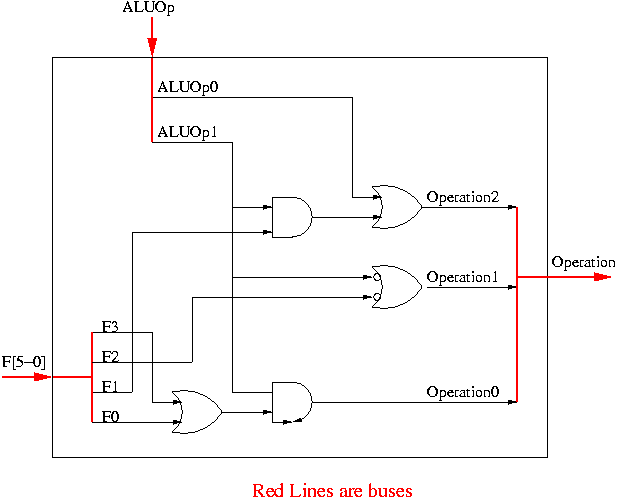
Hence Bnegate is ALUOp0 + (ALUOp1 F1)
Now we apply the same technique to determine when is OP0 asserted and begin by listing the rows where its bit is set.
    ALUOp | Funct
    1 0   | 5 4 3 2 1 0
    ------+------------
    1 x   | x x 0 1 0 1
    1 x   | x x 1 0 1 0
Again looking at all the rows where ALUOp=1x we see
that the two rows where OP0 is asserted are characterized by
just two Function bits
    ALUOp | Funct
    1 0   | 5 4 3 2 1 0
    ------+------------
    1 x   | x x x x x 1
    1 x   | x x 1 x x x
So OP0 is ALUOp1 F0 + ALUOp1 F3
Finally, we determine when is OP1 asserted and once again begin by listing the rows where its bit is one.
    ALUOp | Funct
    1 0   | 5 4 3 2 1 0
    ------+------------
    0 0   | x x x x x x
    x 1   | x x x x x x
    1 x   | x x 0 0 0 0
    1 x   | x x 0 0 1 0
    1 x   | x x 1 0 1 0
Inspection of the 5 rows with ALUOp=1x yields one F bit that distinguishes when OP1 is asserted, namely F2=0. Is this good luck, or well chosen funct values, or wise subset selection by H&P?
    ALUOp | Funct
    1 0   | 5 4 3 2 1 0
    ------+------------
    0 0   | x x x x x x
    x 1   | x x x x x x
    1 x   | x x x 0 x x
Since x 1 in the second row is really 0 1, rows 1 and 2 can be combined to give
	ALUOp | Funct
	1 0   | 5 4 3 2 1 0
	------+------------
	0 x   | x x x x x x
	1 x   | x x x 0 x x
Now we can use the first row to enlarge the scope of the last row
	ALUOp | Funct
	1 0   | 5 4 3 2 1 0
	------+------------
	0 x   | x x x x x x
	x x   | x x x 0 x x
So OP1 = NOT ALUOp1 + NOT F2
The circuit is then easy and is shown on the right.
Our task, illustrated in the diagram below, is to calculate 9 bits, specifically:
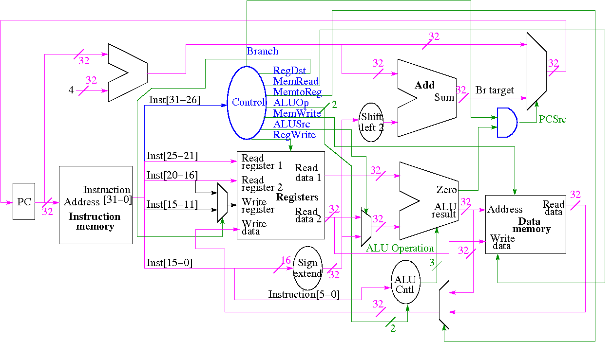
All 9 bits are determined by the opcode. We show the logic diagram after we illustrate the operation of the control logic.
Note that the MIPS instruction set is fairly regular. Most of the fields we need are always in the same place in the instruction (independent of the instruction type).
| MemRead: | Memory delivers the value stored at the specified addr |
| MemWrite: | Memory stores the specified value at the specified addr |
| ALUSrc: | Second ALU operand comes from (reg-file / sign-ext-immediate) |
| RegDst: | Number of reg to write comes from the (rt / rd) field |
| RegWrite: | Reg-file stores the specified value in the specified register |
| PCSrc: | New PC is Old PC+4 / Branch target |
| MemtoReg: | Value written in reg-file comes from (alu / mem) |
We have just seen how to calculate ALUOp, the remaining 7 bits (recall that ALUOp is 2 bits) are described in the table to the right and their uses in controlling the datapath is shown in the picture above.
We are interested in four opcodes.
Do a stage play
volunteers
	add r9,r5,r1 r9=r5+r1   0   5   1   9   0  32
	sub r9,r9,r6            0   9   6   9   0  34
	beq r9,r0,-8            4   9   0   <  -2   >
	slt r1,r9,r0            0   9   0   1   0  42
	lw  r1,102(r2)         35   2   1   <  100  >
	sw  r9,102(r2)
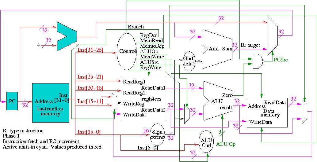
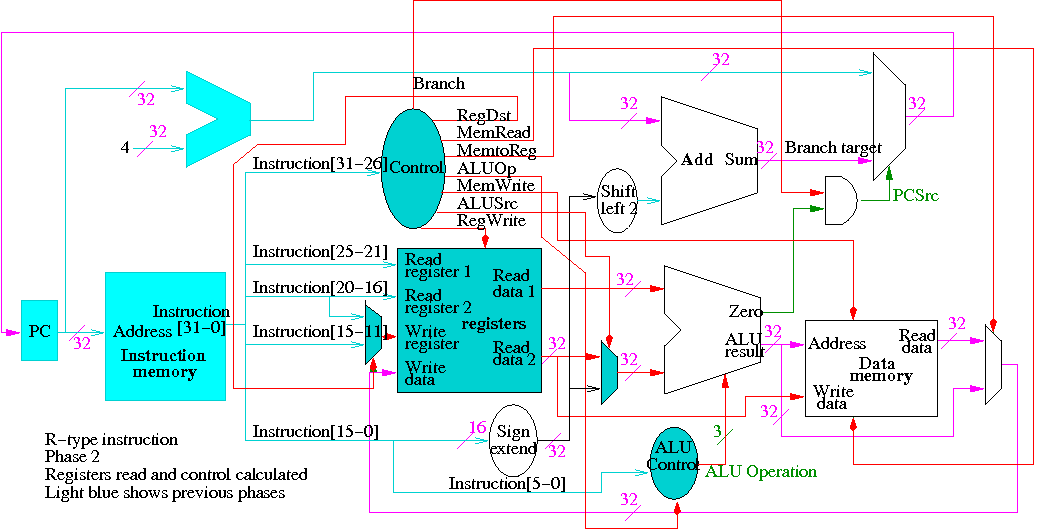
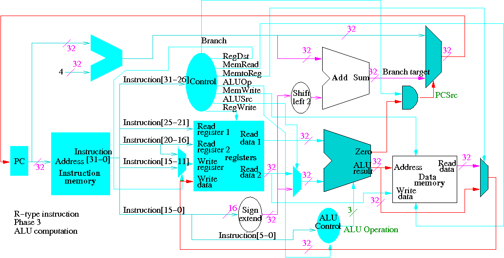
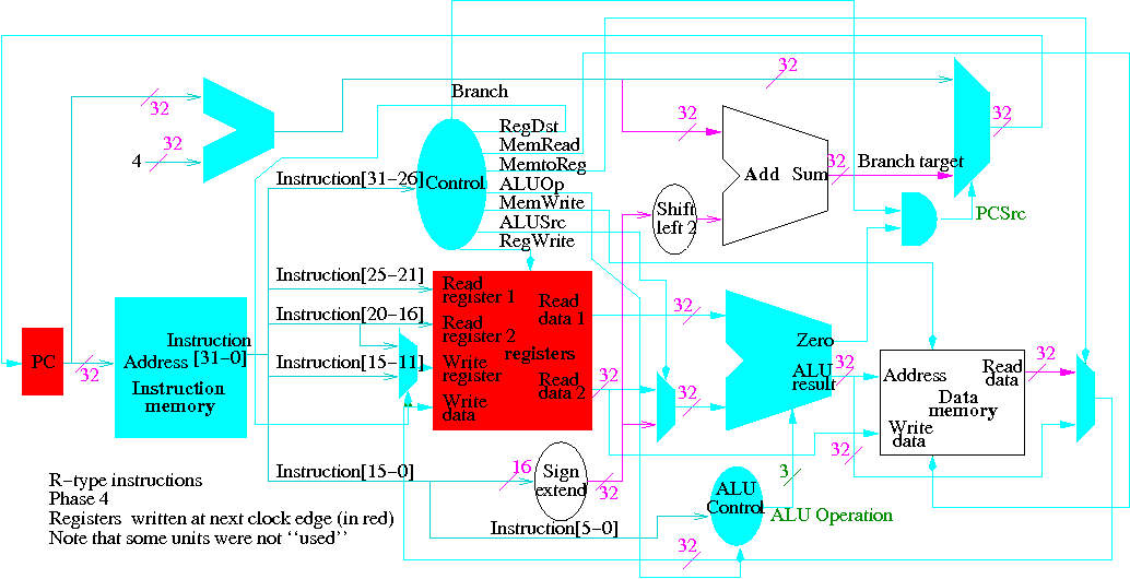
The following figures illustrate the play.
We start with R-type instructions