Start Lecture #3
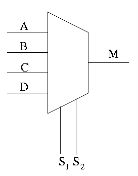
The diagram on the right shows a 4-input MUX.
Construct on the board an equivalent circuit with ANDs and ORs in three ways:
All three of these methods generalize to a mux with 2k input lines, and k select lines.
A 2-way mux is the hardware analogue of if-then-else.
    if S=0
        M=A
    else
        M=B
    endif
A 4-way mux is an if-then-elif-elif-else
    if S1=0 and S2=0
        M=A
    elif S1=0 and S2=1
        M=B
    elif S1=1 and S2=0
        M=C
    else -- S1=1 and S2=1
        M=D
    endif
| S | I0 | I1 | O |
|---|---|---|---|
| 0 | 0 | X | 0 |
| 0 | 1 | X | 1 |
| 1 | X | 0 | 0 |
| 1 | X | 1 | 1 |
Consider a 2-input mux. If the selector is 0, the output is I0 and the value of I1 is irrelevant. Thus, when the selector is 0, I1 is a don't care input. Similarly, when the selector is 1, I0 is a don't care input.
On the right we see the resulting truth table. Recall that without using don't cares the table would have 8 rows since there are three inputs; in this example the use of don't cares reduced the table size by a factor of 2.
The truth table for a 4-input mux has 64 rows, but the use of don't care inputs has a dramatic effect. When the selector is 01 (i.e, S0 is 0 and S1 is 1), the output equals the value of I1 and the other three I's are don't care. A corresponding result occurs for other values of the selector.
Homework: Draw the truth table for a 4-input mux making use of don't care inputs. What size reduction occurred with the don't cares?
Homework:
B.13.
(I am not sure what is meant by hierarchial
;
perhaps modular
).
B.10. (Assume you have constant signals 1 and 0 as well.)
Recall that a don't care output occurs when for some input values (i.e., rows in the truth table), we don't care what the value is for certain outputs.
mux outthese outputs when we have the specified inputs.
How can one construct a 5-way mux?
Construct an 8-way mux and use it as follows.
Can do better by realizing the select lines equalling 5, 6, or 7 are don't cares and hence the 8-way can be customized and would use fewer gates than an 8-way mux.
The idea is to partially automate the algorithmic way you can
produce a circuit diagram (in the sums of product form) from a given
truth table.
Since the form of the circuit is always a bunch of ANDs feeding into
a bunch of ORs, we can manufacture
all the gates in advance
of knowing the desired logic functions and when the functions are
specified, we just need to make the necessary connections from the
ANDs to the ORs.
In essence all possible connections are configured but with
switches that can be open or closed.
| A | B | C | D | E | F |
|---|---|---|---|---|---|
| 0 | 0 | 0 | 0 | 0 | 0 |
| 0 | 0 | 1 | 1 | 0 | 0 |
| 0 | 1 | 0 | 1 | 0 | 0 |
| 0 | 1 | 1 | 1 | 1 | 0 |
| 1 | 0 | 0 | 1 | 0 | 0 |
| 1 | 0 | 1 | 1 | 1 | 0 |
| 1 | 1 | 0 | 1 | 1 | 0 |
| 1 | 1 | 1 | 1 | 0 | 1 |
The description just given is more accurate for a PAL (Programmable Array Logic) than for a PLA, as we shall soon see.
Consider the truth table on the right, which we have seen before. It has three inputs A, B, and C, and three outputs D, E, F.
Below the truth table we see the corresponding logic diagram in sum of products form
Recall how we construct this diagram from the truth table.
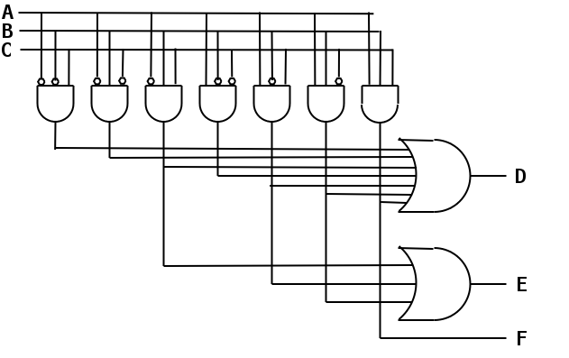
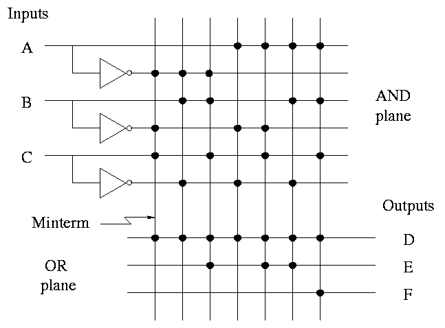
To the right, the above figure is redrawn in a more schematic style.

Finally, a PLA can be redrawn in the more abstract form shown on the right.
Before a PLA is manufactured all the connections are specified. That is, a PLA is specific for a given circuit. Hence the name Programmable Logic Array is somewhat of a misnomer since the device is not programmable by the user.
Homework: B.11 and B.12.
A PAL can be thought of as a PLA in which the final dots are made
by the user.
The manufacturer produces a sea of gates
.
The user programs it to the desired logic function by adding the
dots.
One way to implement a mathematical function (or a java function without side effects) is to perform a table lookup.
A ROM (Read Only Memory) is the analogous way to implement a logic function.
Important: A ROM does not have state.
It is another combinational circuit.
That is, it does not represent memory
.
The reason is that once a ROM is manufactured, the output depends
only on the input.
I realize this sounds wrong, but it is right.
Indeed, we will shortly see that a ROM is like a PLA. Both are structures that can be used to implement a truth table.
The key property of combinational circuits is that the outputs depend only on the inputs. This property (having no state) is false for a RAM chip. The input to a RAM, just like the input to a ROM, is an address. The RAM responds by presenting at its outputs the value CURRENTLY stored at that address. Thus just knowing the input (i.e., the address) is not sufficient for determining the output.
A PROM is a programmable ROM.
That is, you buy the ROM with nothing
in its memory and
then before it is placed in the circuit you load the
memory, and never change it.
This is like a CD-R.
An EPROM is an erasable PROM. It costs more but if you decide to change its memory this is possible (but is slow). This is like a CD-RW.
Normal
EPROMs are erased by some ultraviolet light process.
But EEPROMs (electrically erasable PROMS) are
not as slow and are done electronically.
Flash is a modern EEPROM that is reasonably fast.
All these EPROMS are erasable not writable, i.e. you can't just change one byte to an arbitrary value. (Some modern flash rams can nearly replace true ram and perhaps should not be called EPROMS).
A ROM is similar to PLA
| A | B | C | D | E | F |
|---|---|---|---|---|---|
| 0 | 0 | 0 | 0 | 0 | 0 |
| 0 | 0 | 1 | 1 | 0 | 1 |
| 0 | 1 | 0 | 0 | 1 | 1 |
| 0 | 1 | 1 | 1 | 1 | 0 |
| 1 | 0 | 0 | 1 | 1 | 1 |
| 1 | 0 | 1 | 1 | 1 | 0 |
| 1 | 1 | 0 | 1 | 1 | 0 |
| 1 | 1 | 1 | 1 | 1 | 0 |
muxed outdownstream).
| A | B | C | D | E | F |
|---|---|---|---|---|---|
| 0 | 0 | 0 | 0 | 0 | 0 |
| 0 | 0 | 1 | 1 | 0 | 1 |
| 0 | 1 | 0 | 0 | 1 | 1 |
| 0 | 1 | 1 | 1 | 1 | X |
| 1 | 0 | 0 | 1 | 1 | X |
| 1 | 0 | 1 | 1 | 1 | X |
| 1 | 1 | 0 | 1 | 1 | X |
| 1 | 1 | 1 | 1 | 1 | X |
The top diagram on the right is the full truth table for the following example (from the book). Consider a logic function with three inputs A, B, and C, and three outputs D, E, and F.
The full truth table has 7 minterms (rows with at least one nonzero output).
The middle truth table has the output don't cares included.
| A | B | C | D | E | F |
|---|---|---|---|---|---|
| 0 | 0 | 0 | 0 | 0 | 0 |
| 0 | 0 | 1 | 1 | 0 | 1 |
| 0 | 1 | 0 | 0 | 1 | 1 |
| X | 1 | 1 | 1 | 1 | X |
| 1 | X | X | 1 | 1 | X |
Now do the input don't cares
The resulting truth table is also shown on the right. Note how much smaller it is
These don't cares are important for logic minimization.
Compare the number of gates needed for the full truth table and the
reduced truth table.
There are techniques for minimizing logic, but we will not cover
them.
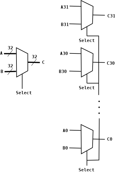
Often we want to consider signals that are wider than a single bit. An array of logic elements is used when each of the individual bits is treated similarly. As we will soon see, sometimes most of the bits are treated similarly, but there are a few exceptions. For example, a 32-bit structure might treat the lob (low order bit) and hob differently from the others. In such a case we would have an array 30 bits wide and two 1-bit structures.
by nnotation.
Skipped.
We will produce logic designs for the integer portion of the MIPS ALU (the floating point operations are more complicated and will not be implemented).
MIPS is a computer architecture widely used in embedded designs.
In the 80s and early 90s, it was quite popular for desktop (or
desk-side) computers.
This was the era of the killer micros
that decimated the
market for minicomputers.
(When I got my DECstation with a MIPS R3000, I think it was the
fastest integer computer at NYU for a short while.)
Much of the design (all of the beginning part) is generic. I will point out when we are tailoring it for MIPS.
Our first goal will be a 1-bit wide structure that computes the AND, OR, and SUM of two 1-bit quantities. For the sum there is actually a third input, CarryIn, and a 2nd output, CarryOut.
Since out basic logic toolkit already includes AND and OR gates, our first real task is a 1-bit adder.
If the final goal was a 1-bit ALU, then we would not have a
CarryIn.
For a multi-bit ALU, the CarryIn for each bit is the CarryOut of the
preceding lower-order bit (e.g., the CarryIn for bit 3 is the
CarryOut from bit 2).
When we don't have a CarryIn, the structure is sometimes called
a half adder
.
Don't treat the name too seriously; it is not half of an adder.
Homework: Draw the logic diagram.