======== START LECTURE #5
========
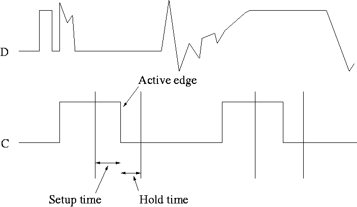
This picture shows the setup and hold times discussed above.
- It is crucial when building circuits with flip flops that D is
stable during the interval between the setup and hold times.
- Note that D is wild outside the critical interval, but that is OK.
- We will not be emphasizing setup and hold requirements in this course.
Homework:
B.18

Registers
A register is basically just an array of D flip-flops.
For example a 32-bit register is an array of 32 D flops.
- Basically just an array of D flip-flops.
particular cycle?
- Introduce another input, the write line.
- The write line is used to ``gate the clock''.
- Clearly if the write line is high forever, the clock input to
the register is passed right along to the D flop and hence the
input to the register is stored in the D flop when the active edge
occurs (for us the falling edge).
- Also clear is that if the write line is low forever, the clock
to the D flop is always low so has no edges and no writing occurs.
- Now we understand what happens if the write line never changes.
What if we want to change the write line (i.e., assert or de-assert it)?
- Assert or deassert the write line while the clock is low.
Changing the Write line when the clock is
low has no effect on the output of the AND and hence does not
effect the clock to the D flop. In particular it does not
introduce any new edges.
- So we change the write line only when the clock is low.
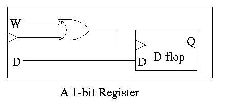
This, however, is not so good! We must have the write line correct
quite a while before the active edge. That is you must know
whether you are writing quite a while in advance.
- Better to arrange everything so that the write line must be
correct when the clock is high (i.e., just before the active
edge).
- Thus we OR the write line with the clock so that it can be
changed when the clock is high without affecting the clock to the
D-flop.

An alternative is to use an active low write line,
i.e. have a W' input.
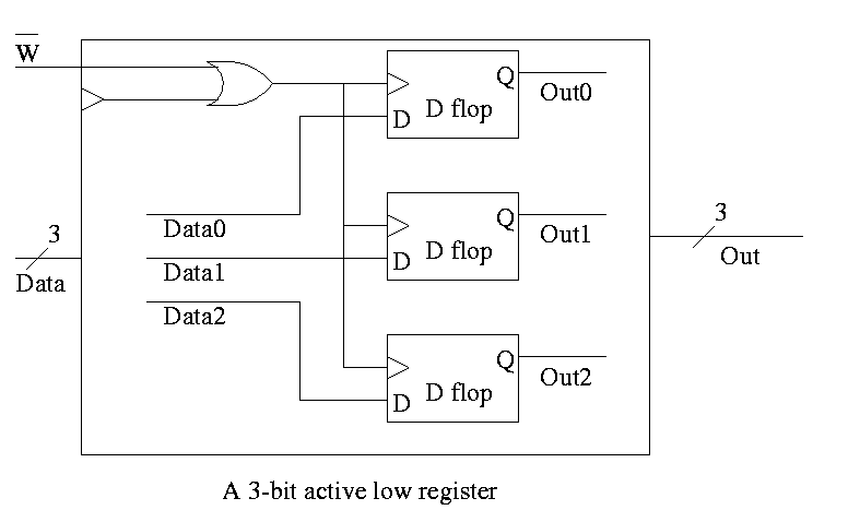
To implement a multibit register, just use multiple D flops.
- Note that the 3-bit Data input is shown both as one 3-bit line and
as three 1-bit lines.
- This dual representation is also used for the 3-bit Out output.

Register File
A register file is just a set of registers, each one numbered.
- To access a register file, you supply reg#, write line (asserted
if a write is to be done), and data (if a write).
- You can read and write same register during one cycle. You read
the old value and then the written value replaces this old value for
subsequent cycles.
- Often have several read and write ports so that several
registers can be read and written during one cycle.
- We will implement 2 read ports and one write port since that is
needed for ALU ops. This is Not adequate for superscalar (or
EPIC) or any other system where more than one operation is to be
calculated each cycle.
Reading From a Register File
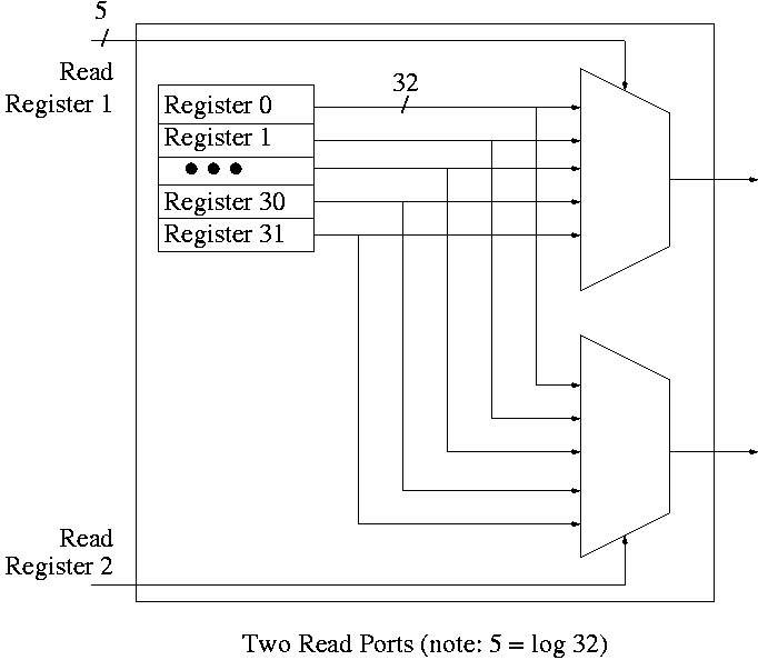 To support reading a register we just need a (big) mux from the
register file to select the correct register.
To support reading a register we just need a (big) mux from the
register file to select the correct register.
- Have one of these big muxes for each read port
- Each big mux is an n to 1 mux, b bits wide; where
- n is the number of registers (32 for MIPS)
- b is the width of each register (32 for MIPS)
- As always we need ceiling(log(n)) bits for selecting which of the
n input to produce.
Writing a Register in a Register File
 To support writing a register we use a decoder on the register number
to determine which
register to write. Note that 3 errors in the book's figure were fixed
To support writing a register we use a decoder on the register number
to determine which
register to write. Note that 3 errors in the book's figure were fixed
- The decoder is log n to n (5 to 32 for MIPS).
- the decoder outputs are numbered 0 to n-1 (NOT n).
- A clock is needed.
Recall that the inputs to a register are W, the write line, D the
data to write (if the write line is asserted), and the clock.
We should perform a write to register r this cycle if the write line
is asserted and the register number specified is r.
The idea is to gate the write line with the output of the decoder.
- The clock to each register is simply the clock input to the
register file.
- The data to each register is simply the write data to the register file.
- The write line to each register is unique.
- The register number is fed to a decoder.
- The rth output of the decoder is asserted if r is the
specified register.
- Hence we wish to write register r if
- The write line to the register file is asserted
- The rth output of the decoder is asserted
- Bingo! We just need an and gate.
Homework: 20
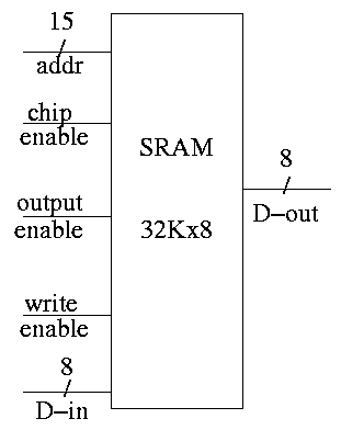
SRAMS and DRAMS
- External interface is on right
- 32Kx8 means it hold 32K words each 8 bits.
- Addr, D-in, and D-out are same as registers. Addr is 15
bits since 2 ^ 15 = 32K. D-out is 8 bits since we have a by 8
SRAM.
- Write enable is similar to the write line (unofficial: it
is a pulse; there is no clock),
- Output enable is for the three state (tri-state) drivers
discussed just below (unofficial).
- Ignore chip enable (perfer not to have all chips enabled
for electrical reasons).
- (Sadly) we will not look inside officially. Following is
unofficial
- Conceptually, an SRAM is like a register file but we can't
use the register file implementation for a large SRAM because
there would be too many wires and the muxes would be too big.
- Two stage decode.
- For a 32Kx8 SRAM would need a 15-32K decoder.
- Instead package the SRAM as eight 512x64 SRAMS.
- Pass 9 bits of the address through a 9-512 decoder and
use these 512 wires to select the appropriate 64-bit word
from each of the sub SRAMS. Use the remaining 6 bits to
select the appropriate bit from each 64-bit word.
- Tri-state buffers (drivers) used instead of a mux.
- I was fibbing when I said that signals always have a 1 or 0.
- However, we will not use tristate logic; we will use muxes.
- DRAM uses a version of the above two stage decode.
- View the memory as an array.
- First select (and save in a ``faster'' memory) an
entire row.
- Then select and output only one (or a few) column(s).
- So can speed up access to elts in same row.
- SRAM and ``logic'' are made from similar technologies but
DRAM technology is quite different.
- So easy to merge SRAM and CPU on one chip (SRAM
cache).
- Merging DRAM and CPU is more difficult but is now
being done.
- Error Correction (Omitted)
Note:
There are other kinds of flip-flops T, J-K. Also one could learn
about excitation tables for each. We will not cover this
material (H&P doesn't either). If interested, see Mano