======== START LECTURE #3
========
Test of XOR symbol ⊕ end of test
Encoder
- Reverse "function" of decoder.
- Not defined for all inputs (exactly one must be 1)
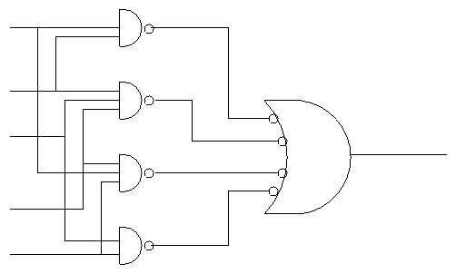
Sneaky way to see that NAND is universal.
- First show that you can get NOT from NAND. Hence we can build
inverters.
- Now imagine that you are asked to do a circuit for some function
with N inputs. Assume you have only one output.
- Using inverters you can get 2N signals the N original and N
complemented.

- Recall that the natural sum of products form is a bunch of ORs
feeding into one AND.

- Naturally you can add pairs of bubbles since they ``cancel''

- But these are all NANDS!!
Half Adder
- Two 1-bit inputs: X and Y
- Two 1-bit outputs S and Co (carry out)
- No carry in
- Draw TT
Homework: Draw logic diagram
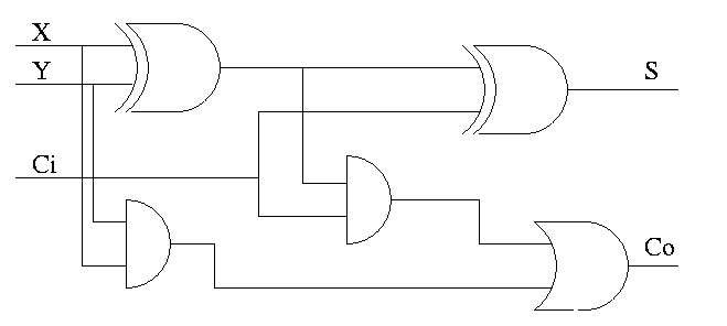
Full Adder
- Three 1-bit inputs: X, Y and Ci.
- Two 1-bit output: S and Co
- S = ``the total number of 1s in X, Y, and Ci is odd''
- Co = #1s is at least 2
Homework:
- Draw TT (8 rows)
- Show S = X XOR Y XOR Ci
- Show Co = XY + (X XOR Y)Ci

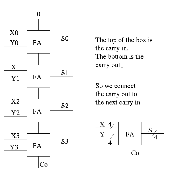
How about 4 bit adder ?

How about an n-bit adder ?
- Linear complexity, i.e. the time for a 64-bit add is twice
that for a 32-bit add.
- Called ripple carry since the carry ripples down the circuit
from the low order bit to the high order bit. This is why the
circuit has linear complexity.
- Faster methods exist. Indeed we will learn one soon.
PLAs--Programmable Logic Arrays
Idea is to make use of the algorithmic way you can look at a TT and
produce a circuit diagram in the sums of product form.
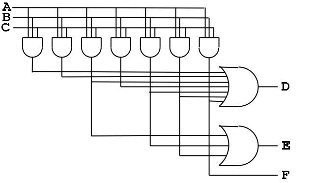
Consider the following TT from the book (page B-13)
     A | B | C || D | E | F
     --+---+---++---+---+--
     O | 0 | 0 || 0 | 0 | 0
     0 | 0 | 1 || 1 | 0 | 0
     0 | 1 | 0 || 1 | 0 | 0
     0 | 1 | 1 || 1 | 1 | 0
     1 | 0 | 0 || 1 | 0 | 0
     1 | 0 | 1 || 1 | 1 | 0
     1 | 1 | 0 || 1 | 1 | 0
     1 | 1 | 1 || 1 | 0 | 1

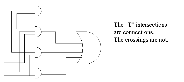
Recall how we construct a circuit from a truth table.
- The circuit is in sum of products form.
- There is a big OR for each output. The OR has one
input for each row that the output is true.
- Since there are 7 rows for which at least one output is true,
there are 7 product terms that will be used in one
or more of the ORs (in fact all seven will be used in D, but that is
special to this example)
- Each of these product terms is called a Minterm
- So we need a bunch of ANDs (in fact, seven, one for each minterm)
taking A, B, C, A', B', and C' as inputs.
- This is called the AND plane and the collection of
ORs mentioned above is called the OR plane.
- At the right is the circuit diagram for the above truth table.

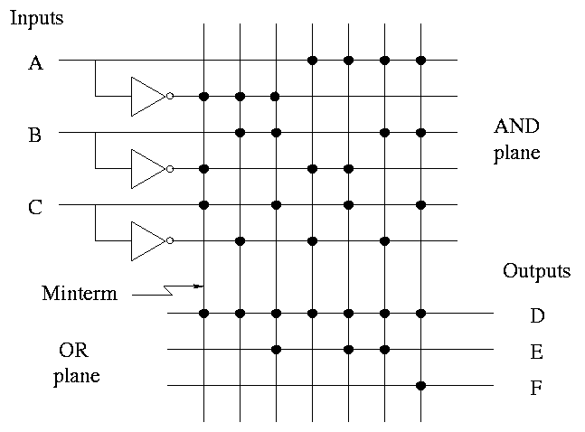
To the right, the above figure is redrawn in a more schematic style.
- This figure shows more clearly the AND plane, the OR plane, and
the minterms.
- Rather than having bubbles (i.e., custom AND gates that invert
certain inputs), we
simply invert each input once and send the inverted signal all the way
accross.
- AND gates are shown as vertical lines; ORs as horizontal.
- Note the dots to represent connections.
- Imagine building a bunch of these but not yet specifying where the
dots go. This would be a generic precursor to a PLA.

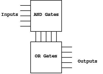
Finally, it can be redrawn in the more abstract form shown on the
right.
Before a PLA is manufactured all the connections are specified.
That is, a PLA is specific for a given circuit. It is somewhat of a
misnomer since it is not programmable by the user.
Homework: B.10 and B.11
Can also have a PAL or Programmable array logic in
which the final dots are made by the user. The manufacturer produces
a ``sea of gates''; the user programs it to the desired logic function
by adding the dots.
ROMs
One way to implement a mathematical (or java) function (without side
effects) is to perform a table lookup.
A ROM (Read Only Memory) is the analogous way to implement a logic
function.
- For a math function f we start with x and get f(x).
- For a ROM with start with the address and get the value stored at
that address.
- Normally math functions are defined for an infinite number of
values, for example f(x) = 3x for all real numbers x
- We can't build an infinite ROM (sorry), so we are only interested
in functions defined for a finite number of values. Today a million
is OK a billion is too big.
- How do we create a ROM for the function f(3)=4, f(6)=20 all other
values don't care?
Simply have the ROM store 4 in address 3 and 20 in address 6.
- Consider a function defined for all n-bit numbers (say n=20) and
having a k-bit output for each input.
- View an n-bit input as n 1-bit inputs.
- View a k-bit output as k 1-bit outputs.
- Since there are 2^n possible inputs and each requires a k 1-bit output,
there are a total of (2^n)k bits of output, i.e. the ROM must hold
(2^n)k bits.
- Now consider a truth table with n inputs and k outputs.
The total number of output bits is again (2^n)k (2^n rows and k output
columns).
- Thus the ROM implements a truth table, i.e. is a logic function.
Important: A ROM does not have state. It is
another combinational circuit. That is, it does not represent
``memory''. The reason is that once a ROM is manufactured, the output
depends only on the input. I realize this sounds wrong, but it is right.
A PROM
is a programmable ROM. That is you buy the ROM with ``nothing'' in
its memory and then before
it is placed in the circuit you load the memory, and never change it.
This is like a CD-R.
An EPROM is an erasable PROM. It costs more
but if you decide to change its memory this is possible (but is slow).
This is like a CD-RW.
``Normal'' EPROMs are erased by some ultraviolet light process. But
EEPROMs (electrically erasable PROMS) are faster and
are done electronically.
All these EPROMS are erasable not writable, i.e. you can't just change
one bit.
A ROM is similar to PLA
- Both can implement any truth table, in principle.
- A 2Mx8 ROM can really implment any truth table with 21 inputs
(2^21=2M) and 8 outputs.
- It stores 2M bytes
- In ROM-speak, it has 21 address pins and 8 data pins
- A PLA with 21 inputs and 8 outputs might need to have 2M minterms
(AND gates).
- The number of minterms depends on the truth table itself.
- For normal TTs with 21 inputs the number of minterms is MUCH
less than 2^21.
- The PLA is manufactured with the number of minterms needed
- Compare a PAL with a PROM
- Both can in principle implement any TT
- Both are user programmable
- A PROM with n inputs and k outputs can implement any TT with n
inputs and k outputs.
- A PAL that you buy does not have enough gates for all
possibilities since most TTs with n inputs and k outputs don't
require nearly (2^n)k gates.
Don't Cares
- Sometimes not all the input and output entries in a TT are
needed. We indicate this with an X and it can result in a smaller
truth table.
- Input don't cares.
- The output doesn't depend on all inputs, i.e. the output has
the same value no matter what value this input has.
- We saw this when we did muxes.
- Output don't cares
- For some input values, either output is OK.
- This input combination is impossible.
- For this input combination, the given output is not used
(perhaps it is ``muxed out'' downstream).
Example (from the book). Consider a logic function with three inputs
A, B, and C, and three outputs D, E, and F.
- If A or C is true, then D is true (independent of B).
- If A or B is true, then E is true (independent of C).
- F is true if exactly one of the inputs is true, but we don't care
about the value of F if both D and E are true
Full truth table
     A   B   C || D   E   F
     ----------++----------
     0   0   0 || 0   0   0
     0   0   1 || 1   0   1
     0   1   0 || 0   1   1
     0   1   1 || 1   1   0
     1   0   0 || 1   1   1
     1   0   1 || 1   1   0
     1   1   0 || 1   1   0
     1   1   1 || 1   1   1
This has 7 minterms.
Put in the output don't cares
     A   B   C || D   E   F
     ----------++----------
     0   0   0 || 0   0   0
     0   0   1 || 1   0   1
     0   1   0 || 0   1   1
     0   1   1 || 1   1   X
     1   0   0 || 1   1   X
     1   0   1 || 1   1   X
     1   1   0 || 1   1   X
     1   1   1 || 1   1   X
Now do the input don't cares
- B=C=1 ==> D=E=11 ==> F=X ==> A=X
- A=1 ==> D=E=11 ==> F=X ==> B=C=X
     A   B   C || D   E   F
     ----------++----------
     0   0   0 || 0   0   0
     0   0   1 || 1   0   1
     0   1   0 || 0   1   1
     X   1   1 || 1   1   X
     1   X   X || 1   1   X
These don't cares are important for logic minimization. Compare the
number of gates needed for the full TT and the reduced TT. There are
techniques for minimizing logic, but we will not cover them.

