Computer Systems Design
Appendix B: Logic Design
Homework: Read B1
B.2: Gates, Truth Tables and Logic Equations
Homework: Read B2
Digital ==> Discrete
Primarily (but NOT exclusively) binary at the hardware level
Use only two voltages--high and low.
- This hides a great deal of engineering.
- Must make sure not to sample the signal when not in one of these two states.
- Sometimes it is just a matter of waiting long enough
(determines the clock rate i.e. how many megahertz).
- Other times it is worse and you must avoid glitches.
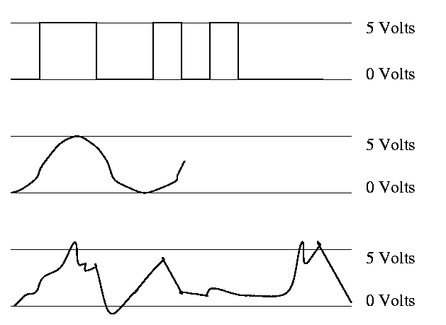
- Oscilloscope traces shown on the right.
- Vertical axis is voltage; horizontal axis is time.
- Square wave--the ideal. How we think of circuits
- (Poorly drawn) Sine wave
- Actual wave
- Non-zero rise times and fall times
- Overshoots and undershoots
- Glitches
Since this is not an engineering course, we will ignore these
issues and assume square waves.
In English digital implies 10 (based on digit, i.e. finger),
but not in computers.
Bit = Binary digIT
Instead of saying high voltage and low voltage, we say true and false
or 1 and 0 or asserted and deasserted.
0 and 1 are called complements of each other.
A logic block can be thought of as a black box that takes signals in
and produces signals out. There are two kinds of blocks
- Combinational (or combinatorial)
- Does NOT have memory elements.
- Is simpler than circuits with memory since the outputs are a
function of the inputs. That is, if the same inputs are presented on
Monday and Tuesday, the same outputs will result.
- Sequential
- Contains memory.
- The current value in the memory is called the state of the block.
- The output depends on the input AND the state.
We are doing combinational blocks now. Will do sequential blocks
later (in a few lectures).
TRUTH TABLES
Since combinatorial logic has no memory, it is simply a function from
its inputs to its outputs. A
Truth Table has as columns all inputs
and all outputs. It has one row for each possible set of input values
and the output columns have the output for that input. Let's start
with a really simple case a logic block with one input and one output.
There are two columns (1 + 1) and two rows (2**1).
In  Out
0   ?
1   ?
How many possible truth tables are there?
How many different truth tables are there for a ``one in one out''
logic block?
Just 4: The constant functions 1 and 0, the identity, and an inverter
(pictures in a few minutes). There are two `?'s in the above table;
each can be a 0 or 1 so 2**2 possibilities.
OK. Now how about two inputs and 1 output.
Three columns (2+1) and 4 rows (2**2).
In1 In2  Out
0   0    ?
0   1    ?
1   0    ?
1   1    ?
How many are there? It is just the number ways can you fill in the
output entries, i.e. the question marks. There are 4 output entries
so answer is 2**4=16.
How about 2 in and 8 out?
- 10 cols
- 4 rows
- 2**(4*8)=4 billion possible
3 in and 8 out?
- 11 cols
- 8 rows
- 2**(8**8)=2**64 possible
n in and k out?
- n+k cols
- 2**n rows
- 2**([2**n]*k) possible
Gets big fast!
Boolean algebra
Certain logic functions (i.e. truth tables) are quite common and
familiar.
We use a notation that looks like algebra to express logic functions and
expressions involving them.
The notation is called Boolean algebra in honor of
George Boole.
A Boolean value is a 1 or a 0.
A Boolean variable takes on Boolean values.
A Boolean function takes in boolean variables and produces boolean values.
- The (inclusive) OR Boolean function of two variables. Draw its
truth table. This is written + (e.g. X+Y where X and Y are Boolean
variables) and often called the logical sum. (Three out of four
output values in the truth table look right!)
- AND. Draw TT. Called logical product and written as a centered dot
(like product in regular algebra). All four values look right.
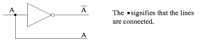
- NOT. Draw TT. This is a unary operator (One argument, not two
as above; functions with two inputs are called binary). Written A with a bar
over it. I will use ' instead of a bar as it is easier for me to type
in html.
- Exclusive OR (XOR). Written as + with a circle around it. True if
exactly one input is true (i.e., true XOR true = false). Draw TT.
Homework:
Consider the Boolean function of 3 boolean variables that is true
if and only if exactly 1 of the three variables is true. Draw the TT.
Some manipulation laws. Remember this is Boolean ALGEBRA.
Identity:
-
A+0 = 0+A = A
-
A.1 = 1.A = A
-
(using . for and)
Inverse:
- A+A' = A'+A = 1
- A.A' = A'.A = 0
- (using ' for not)
Both + and . are commutative so my identity and inverse examples
contained redundancy.
The name inverse law is somewhat funny since you
Add the inverse and get the identity for Product
or Multiply by the inverse and get the identity for Sum.
Associative:
- A+(B+C) = (A+B)+C
- A.(B.C)=(A.B).C
Due to the associative law we can write A.B.C since either order of
evaluation gives the same answer. Similarly we can write A+B+C.
We often elide the . so the product associative law is A(BC)=(AB)C.
So we better not have three variables A, B, and AB. In fact, we
normally use one letter variables.
Distributive:
- A(B+C)=AB+AC
- A+(BC)=(A+B)(A+C)
- Note that BOTH distributive laws hold UNLIKE ordinary arithmetic.
How does one prove these laws??
- Simple (but long). Write the TTs for each and see that the outputs
are the same.
- Prove the first distributive law on the board.
Homework: Prove the second distributive law.
Let's do (on the board) the examples on pages B-5 and B-6.
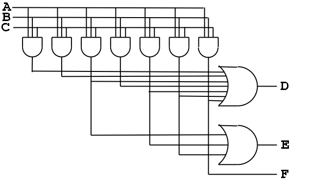
Consider a logic function with three inputs A, B, and C; and three
outputs D, E, and F defined as follows: D is true if at least one
input is true, E if exactly two are true, and F if all three are true.
(Note that by ``if'' we mean ``if and only if''.
Draw the truth table.
Show the logic equations.
- For E first use the obvious method of writing one condition
for each 1-value in the E column i.e.
(A'BC) + (AB'C) + (ABC')
- Observe that E is true if two (but not three) inputs are true,
i.e.,
(AB+AC+BC) (ABC)' (using . higher precedence than +)
======== START LECTURE #2
========
The first way we solved part E shows that any logic function
can be written using just AND, OR, and NOT. Indeed, it is in a nice
form.
Called two levels of logic since it is a sum of products of
just inputs and their compliments. That is it can be computed in just
two time steps (assuming you already have the compliments). First you
take all the needed products and then all the sums
DeMorgan's laws:
- (A+B)' = A'B'
- (AB)' = A'+B'
You prove DM laws with TTs. Indeed that is ...
Homework: B.6 on page B-45.
Do beginning of HW on the board.
With DM (DeMorgan's Laws) we can do quite a bit without resorting to
TTs. For example one can show that the two expressions for E in the
example above (page B-6) are equal. Indeed that is
Homework: B.7 on page B-45
Do beginning of HW on board.
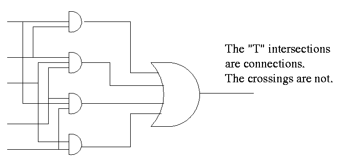
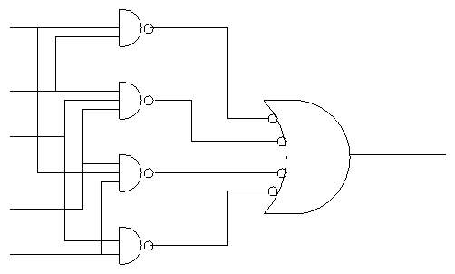
GATES
Gates implement basic logic functions: AND OR NOT XOR Equivalence
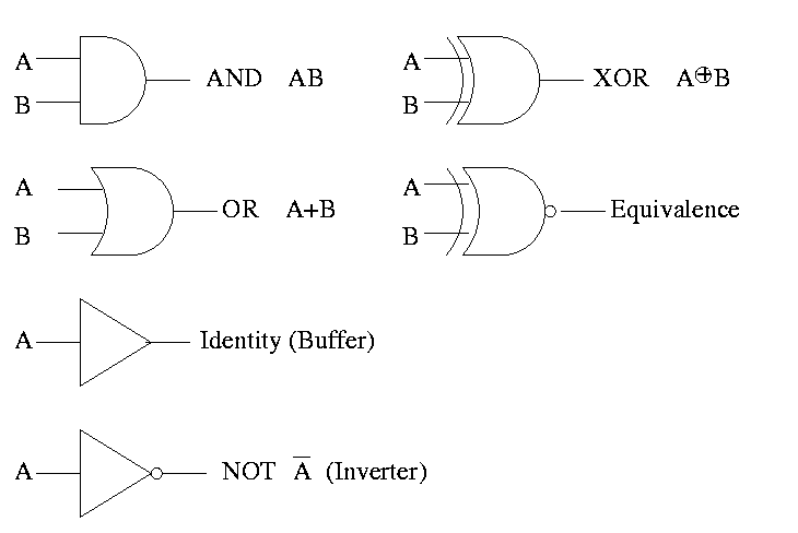
Often omit the inverters and draw the little circles at the input or
output of the other gates (AND OR). These little circles are
sometimes called bubbles.
This explains why the inverter is drawn as a buffer with a bubble.
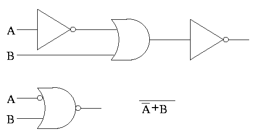
Show why the picture for equivalence is the negation of XOR, i.e (A
XOR B)' is AB + A'B'
(A XOR B)' =
(A'B+AB')' =
(A'B)' (AB')' =
(A''+B') (A'+B'') =
(A + B') (A' + B) =
AA' + AB + B'A' + B'B =
0   + AB + B'A' + 0 =
AB + A'B'
Homework: B.2 on page B-45 (I previously did the first part
of this homework).
Homework: Consider the Boolean function of 3 boolean vars
(i.e. a three input function) that is true if and only if exactly 1 of
the three variables is true. Draw the TT. Draw the logic diagram
with AND OR NOT. Draw the logic diagram with AND OR and bubbles.
A set of gates is called universal if these gates are
sufficient to generate all logic functions.
-
We have seen that any logic function can be constructed from AND OR
NOT. So this triple is universal.
-
Are there any pairs that are universal?
Ans: Sure, A+B = (A'B')' so can get OR from AND and NOT. Hence the
pair AND NOT is universal
Similarly, can get AND from OR and NOT and hence the pair OR NOT
is universal
-
Could there possibly be a single function that is universal all by
itself?
AND won't work as you can't get NOT from just AND
OR won't work as you can't get NOT from just OR
NOT won't work as you can't get AND from just NOT.
-
But there indeed is a universal function! In fact there are two.
NOR (NOT OR) is true when OR is false. Do TT.
NAND (NOT AND) is true when AND is false. Do TT.
Draw two logic diagrams for each, one from the definition and an
equivalent one with bubbles.
Theorem
A 2-input NOR is universal and
a 2-input NAND is universal.
Proof
We must show that you can get A', A+B, and AB using just a two input
NOR.
- A' = A NOR A
- A+B = (A NOR B)' (we can use ' by above)
- AB = (A' OR B')'
Homework: Show that a 2-input NAND is universal.
Can draw NAND and NOR each two ways (because (AB)' = A' + B')
We have seen how to get a logic function from a TT. Indeed we can
get one that is just two levels of logic. But it might not be the
simplest possible. That is, we may have more gates than are necessary.
Trying to minimize the number of gates is NOT trivial. Mano covers
the topic of gate minimization in detail. We will not cover it in
this course. It is not in H&P. I actually like it but must admit
that it takes a few lectures to cover well and it not used much in
practice since it is algorithmic and is done automatically by CAD
tools.
Minimization is not unique, i.e. there can be two or more minimal
forms.
Given A'BC + ABC + ABC'
Combine first two to get BC + ABC'
Combine last two to get A'BC + AB
Sometimes when building a circuit, you don't care what the output is
for certain input values. For example, that input combination might
be known not to occur. Another example occurs when, for some
combination of input values, a later part of the circuit will ignore
the output of this part. These are called don't care
outputs situations. Making use of don't cares can reduce the
number of gates needed.
Can also have don't care inputs
when, for certain values of a subset of the inputs, the output is
already determined and you don't have to look at the remaining
inputs. We will see a case of this in the very next topic, multiplexors.
An aside on theory
Putting a circuit in disjunctive normal form (i.e. two levels of
logic) means that every path from the input to the output goes through
very few gates. In fact only two, an OR and an AND. Maybe we should
say three since the AND can have a NOT (bubble). Theorticians call
this number (2 or 3 in our case) the depth of the circuit.
Se we see that every logic function can be implemented with small
depth. But what about the width, i.e., the number of gates.
The news is bad. The parity function takes n inputs
and gives TRUE if and only if the number of TRUE inputs is odd.
If the depth is fixed (say limited to 3), the number of gates needed
for parity is exponential in n.
B.3 COMBINATIONAL LOGIC
Homework:
Read B.3.
Generic Homework:
Read sections in book corresponding to the lectures.
Multiplexor
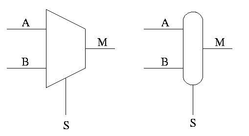
Often called a mux or a selector
Show equiv circuit with AND OR
Hardware if-then-else
    if S=0
        M=A
    else
        M=B
    endif
Can have 4 way mux (2 selector lines)
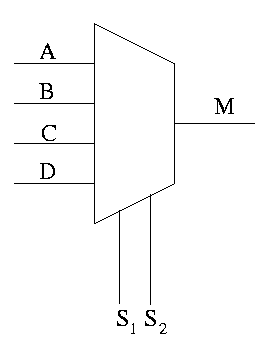
This is an if-then-elif-elif-else
   if S1=0 and S2=0
        M=A
    elif S1=0 and S2=1
        M=B
    elif S1=1 and S2=0
        M=C
    else -- S1=1 and S2=1
        M=D
    endif
Do a TT for 2 way mux. Redo it with don't care values.
Do a TT for 4 way mux with don't care values.
Homework:
B.12.
B.5 (Assume you have constant signals 1 and 0 as well.)
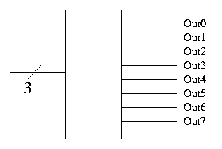
Decoder
- Note the ``3'' with a slash, which signifies a three bit input.
This notation represents three (1-bit) wires.
- A decoder with n input bits, produces 2^n output bits.
- View the input as ``k written an n-bit binary number'' and
view the output as 2^n bits with the k-th bit set and all the
other bits clear.
- Implement on board with AND/OR.
- Why do we use decoders and encoders?
- The encoded form takes (MANY) fewer bits so is better for
communication.
- The decoded form is easier to work with in hardware since
there is no direct way to test if 8 wires represent a 5
(101). You would have to test each wire. But it easy to see
if the encoded form is a five (00100000)
Encoder
- Reverse "function" of decoder.
- Not defined for all inputs (exactly one must be 1)
Sneaky way to see that NAND is universal.
- First show that you can get NOT from NAND. Hence we can build
inverters.
- Now imagine that you are asked to do a circuit for some function
with N inputs. Assume you have only one output.
- Using inverters you can get 2N signals the N original and N
complemented.
- Recall that the natural sum of products form is a bunch of ORs
feeding into one AND.
- Naturally you can add pairs of bubbles since they ``cancel''
- But these are all NANDS!!
Half Adder
- Two 1-bit inputs: X and Y
- Two 1-bit outputs S and Co (carry out)
- No carry in
- Draw TT
Homework: Draw logic diagram
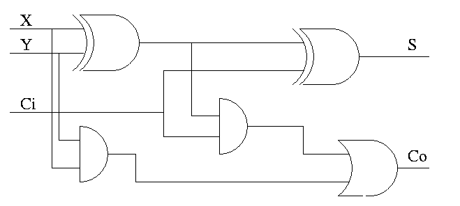
Full Adder
- Three 1-bit inputs: X, Y and Ci.
- Two 1-bit output: S and Co
- S = ``the total number of 1s in X, Y, and Ci is odd''
- Co = #1s is at least 2
Homework:
- Draw TT (8 rows)
- Show S = X XOR Y XOR Ci
- Show Co = XY + (X XOR Y)Ci
How about 4 bit adder ?
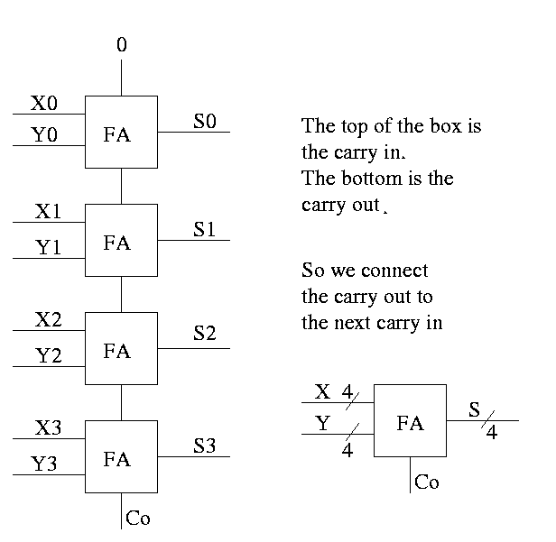
How about an n-bit adder ?
- Linear complexity, i.e. the time for a 64-bit add is twice
that for a 32-bit add.
- Called ripple carry since the carry ripples down the circuit
from the low order bit to the high order bit. This is why the
circuit has linear complexity.
- Faster methods exist. Indeed we will learn one soon.
PLAs--Programmable Logic Arrays
Idea is to make use of the algorithmic way you can look at a TT and
produce a circuit diagram in the sums of product form.
Consider the following TT from the book (page B-13)
     A | B | C || D | E | F
     --+---+---++---+---+--
     O | 0 | 0 || 0 | 0 | 0
     0 | 0 | 1 || 1 | 0 | 0
     0 | 1 | 0 || 1 | 0 | 0
     0 | 1 | 1 || 1 | 1 | 0
     1 | 0 | 0 || 1 | 0 | 0
     1 | 0 | 1 || 1 | 1 | 0
     1 | 1 | 0 || 1 | 1 | 0
     1 | 1 | 1 || 1 | 0 | 1
- Recall how we construct a circuit from a truth table.
- The circuit is in sum of products form.
- There is a big OR for each output. The OR has one
input for each row that the output is true.
- Since there are 7 rows for which at least one output is true,
there are 7 product terms that will be used in one
or more of the ORs (in fact all seven will be used in D, but that is
special to this example)
- Each of these product terms is called a Minterm
- So we need a bunch of ANDs (in fact, seven, one for each minterm)
taking A, B, C, A', B', and C' as inputs.
- This is called the AND plane and the collection of
ORs mentioned above is called the OR plane.
Here is the circuit diagram for this truth table.
Here it is redrawn in a more schmatic style.
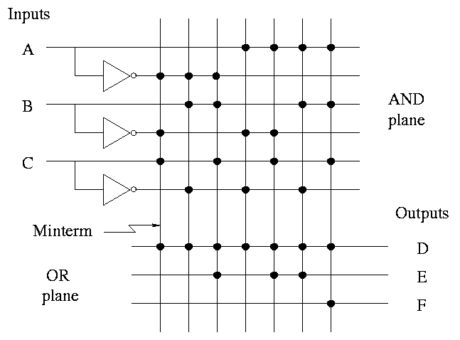
- This figure shows more clearly the AND plane, the OR plane, and
the minterms.
- Rather than having bubbles (i.e., custom AND gates that invert
certain inputs), we
simply invert each input once and send the inverted signal all the way
accross.
- AND gates are shown as vertical lines; ORs as horizontal.
- Note the dots to represent connections.
- Imagine building a bunch of these but not yet specifying where the
dots go. This would be a generic precurson to a PLA.
Finally, it can be redrawn in a more abstract form.
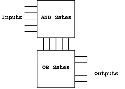
Before a PLA is manufactured all the connections are specified.
That is, a PLA is specific for a given circuit. It is somewhat of a
misnomer since it is notprogrammable by the user
Homework: B.10 and B.11
Can also have a PAL or Programmable array logic
in which the final dots are specified
by the user. The manufacturer produces a ``sea of gates''; the user
programs it to the desired logic function by adding the dots.
ROMs
One way to implement a mathematical (or C) function (without side
effects) is to perform a table lookup.
A ROM (Read Only Memory) is the analogous way to implement a logic
function.
- For a math function f we start with x and get f(x).
- For a ROM with start with the address and get the value stored at
that address.
- Normally math functions are defined for an infinite number of
values, for example f(x) = 3x for all real numbers x
- We can't build an infinite ROM (sorry), so we are only interested
in functions defined for a finite number of values. Today a million
is OK a billion is too big.
- How do we create a ROM for the function f(3)=4, f(6)=20 all other
values don't care?
Simply have the ROM store 4 in address 3 and 20 in address 6.
- Consider a function defined for all n-bit numbers (say n=20) and
having a k-bit output for each input.
- View an n-bit input as n 1-bit inputs.
- View a k-bit output as k 1-bit outputs.
- Since there are 2^n possible inputs and each requires a k 1-bit output,
there are a total of (2^n)k bits of output, i.e. the ROM must hold
(2^n)k bits.
- Now consider a truth table with n inputs and k outputs.
The total number of output bits is again (2^n)k (2^n rows and k output
columns).
- Thus the ROM implements a truth table, i.e. is a logic function.
Important: A ROM does not have state. It is
another combinational circuit. That is, it does not represent
``memory''. The reason is that once a ROM is manufactured, the output
depends only on the input.
A PROM
is a programmable ROM. That is you buy the ROM with ``nothing'' in
its memory and then before
it is placed in the circuit you load the memory, and never change it.
This is like a CD-R.
An EPROM is an erasable PROM. It costs more
but if you decide to change its memory this is possible (but is slow).
This is like a CD-RW.
``Normal'' EPROMs are erased by some ultraviolet light process. But
EEPROMs (electrically erasable PROMS) are faster and
are done electronically.
All these EPROMS are erasable not writable, i.e. you can't just change
one bit.
A ROM is similar to PLA
- Both can implement any truth table, in principle.
- A 2Mx8 ROM can really implment any truth table with 21 inputs
(2^21=2M) and 8 outputs.
- It stores 2M bytes
- In ROM-speak, it has 21 address pins and 8 data pins
- A PLA with 21 inputs and 8 outputs might need to have 2M minterms
(AND gates).
- The number of minterms depends on the truth table itself.
- For normal TTs with 21 inputs the number of minterms is MUCH
less than 2^21.
- The PLA is manufactured with the number of minterms needed
- Compare a PAL with a PROM
- Both can in principle implement any TT
- Both are user programmable
- A PROM with n inputs and k outputs can implement any TT with n
inputs and k outputs.
- A PAL that you buy does not have enough gates for all
possibilities since most TTs with n inputs and k outputs don't
require nearly (2^n)k gates.
Don't Cares
- Sometimes not all the input and output entries in a TT are
needed. We indicate this with an X and it can result in a smaller
truth table.
- Input don't cares.
- The output doesn't depend on all inputs, i.e. the output has
the same value no matter what value this input has.
- We saw this when we did muxes
- Output don't cares
- For some input values, either output is OK.
- This input combination is impossible.
- For this input combination, the given output is not used
(perhaps it is ``muxed out'' downstream)
Example (from the book):
- If A or C is true, then D is true (independent of B).
- If A or B is true, then E is true.
- F is true if exactly one of the inputs is true, but we don't care
about the value of F if both D and E are true
Full truth table
     A   B   C || D   E   F
     ----------++----------
     0   0   0 || 0   0   0
     0   0   1 || 1   0   1
     0   1   0 || 0   1   1
     0   1   1 || 1   1   0
     1   0   0 || 1   1   1
     1   0   1 || 1   1   0
     1   1   0 || 1   1   0
     1   1   1 || 1   1   1
This has 7 minterms.
Put in the output don't cares
     A   B   C || D   E   F
     ----------++----------
     0   0   0 || 0   0   0
     0   0   1 || 1   0   1
     0   1   0 || 0   1   1
     0   1   1 || 1   1   X
     1   0   0 || 1   1   X
     1   0   1 || 1   1   X
     1   1   0 || 1   1   X
     1   1   1 || 1   1   X
Now do the input don't cares
- B=C=1 ==> D=E=11 ==> F=X ==> A=X
- A=1 ==> D=E=11 ==> F=X ==> B=C=X
     A   B   C || D   E   F
     ----------++----------
     0   0   0 || 0   0   0
     0   0   1 || 1   0   1
     0   1   0 || 0   1   1
     X   1   1 || 1   1   X
     1   X   X || 1   1   X
These don't cares are important for logic minimization. Compare the
number of gates needed for the full TT and the reduced TT. There are
techniques for minimizing logic, but we will not cover them.
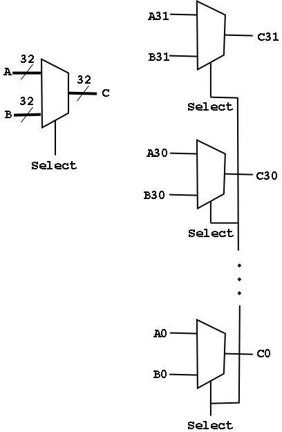
Arrays of Logic Elements
- Do the same thing to many signals
- Draw thicker lines and use the ``by n'' notation.
- Diagram below shows a 32-bit 2-way mux and an implementation with 32
1-bit, 2-way muxes.
- A Bus is a collection of data lines treated
as a single logical (n-bit) value.
- Use an array of logic elements to process a bus.
For example, the above mux switches between 2 32-bit buses.
*** Big Change Coming ***
Sequential Circuits, Memory, and State
Why do we want to have state?
- Memory (i.e. ram not just rom or prom)
- Counters
- Reducing gate count
- Multiplier would be quadradic in comb logic.
- With sequential logic (state) can do in linear.
- What follows is unofficial (i.e. too fast to
understand)
- Shift register holds partial sum
- Real slick is to share this shift reg with
multiplier
- We will do this circuit later in the course
Assume you have a real OR gate. Assume the two inputs are both
zero for an hour. At time t one input becomes 1. The output will
OSCILLATE for a while before settling on exactly 1. We want to be
sure we don't look at the answer before its ready.
B.4: Clocks
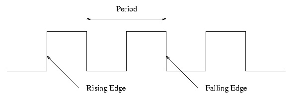
Frequency and period
- Hertz (Hz), Megahertz, Gigahertz vs. Seconds, Microseconds,
Nanoseconds
- Old (descriptive) name for Hz is cycles per second (CPS)
- Rate vs. Time
Edges
- Rising Edge; falling edge
- We use edge-triggered logic
- State changes occur only on a clock edge
- Will explain later what this really means
- One edge is called the Active edge
- The edge (rising or falling) on which changes occur
- Choice is technology dependent
- Sometimes trigger on both edges (e.g., RAMBUS or DDR memory)
Synchronous system
Now we are going to add state elements to the combinational
circuits we have been using previously.
Remember that a combinational/combinatorial circuits has its outpus
determined by its input, i.e. combinatorial circuits do not contain
state.
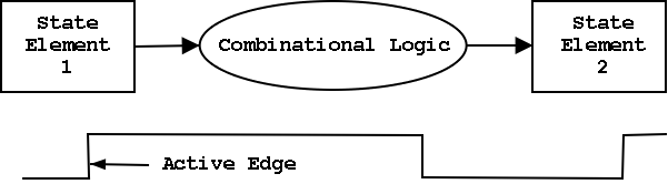
State elements include state (naturally).
- i.e., memory
- state-elements have clock as an input
- can change state only at active edge
- produce output Always; based on current state
- all signals that are written to state elements must be valid at
the time of the active edge.
- For example, if cycle time is 10ns make sure combinational circuit
used to compute new state values completes in 10ns
- So state elements change on active edge, comb circuit
stabilizes between active edges.
- Think of registers or memory as state elements.
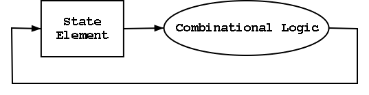
- Can have loops like at the right.
- A loop like this is a cycle of the computer.
B.5: Memory Elements
We want edge-triggered clocked memory and will only use
edge-triggered clocked memory in our designs. However we get
there by stages. We first show how to build unclocked
memory; then using unclocked memory we build
level-sensitive clocked memory; finally from
level-sensitive clocked memory we build edge-triggered
clocked memory.
Unclocked Memory
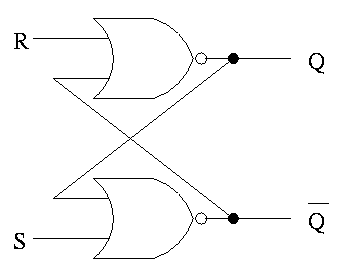
S-R latch (set-reset)
- ``Cross-coupled'' nor gates
- Don't assert both S and R at once
- When S is asserted (i.e., S=1 and R=0)
- the latch is Set (that's why it is called S)
- Q becomes true (Q is the output of the latch)
- Q' becomes false (Q' is the complemented output)
- When R is asserted
- the latch is Reset
- Q becomes false
- Q' becomes true
- When neither one is asserted
- The latch remains the same, i.e. Q and Q' stay as they
were
- This is the memory aspect
Clocked Memory: Flip-flops and latches
The S-R latch defined above is not clocked memory. Unfortunately the
terminology is not perfect.
For both flip-flops and
latches the output equals the value stored in the
structure. Both have an input and an output (and the complemented
output) and a clock input as well. The clock determines when the
internal value is set to the current input. For a latch, the change
occurs whenever the clock is asserted (level sensitive). For a
flip-flop, the change occurs at the active edge.
D latch
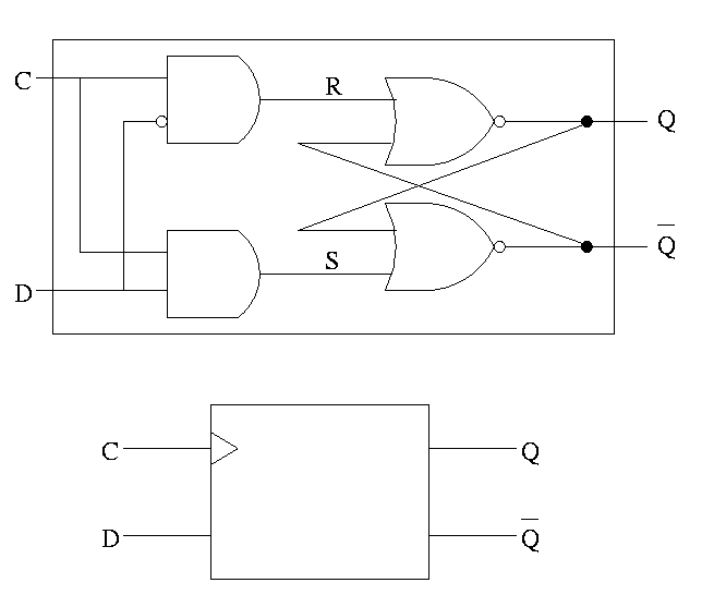
The D is for data
- The left part uses the clock.
- When the clock is low, both R and S are forced low.
- When the clock is high, S=D and R=D' so the value store is D.
- Output changes when input changes and the clock is asserted.
- Level sensitive rather than edge triggered.
- Sometimes called a transparent latch.
- We won't use these in designs.
- The right hand part of the circuit is the S-R (unclocked) latch we
just constructed.
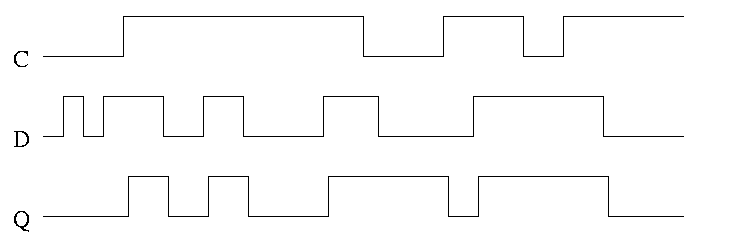
In the traces below notice how the output follows the input when the
clock is high and remains constant when the clock is low. We assume
the stored value is initially low.
D or Master-Slave Flip-flop
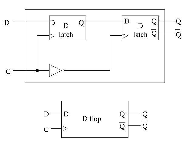
This was our goal. We now have an edge-triggered, clocked memory.
- Built from D latches, which are transparent
- The result is Not transparent
- Changes on the active edge
- This one has the falling edge as active edge
- Sometimes called a master-slave flip-flop
- Note substructures with letters reused
having different meaning (block structure a la algol)
- Master latch (the left one) is set during the time clock is
asserted.
Remember that the latch is transparent, i.e. follows
its input when its clock is asserted. But the second
latch is ignoring its input at this time. When the
clock falls, the 2nd latch pays attention and the
first latch keeps producing whatever D was at
fall-time.
- Actually D must remain constant for some time around
the active edge.
- The set-up time before the edge
- The hold time after the edge
- See diagram below
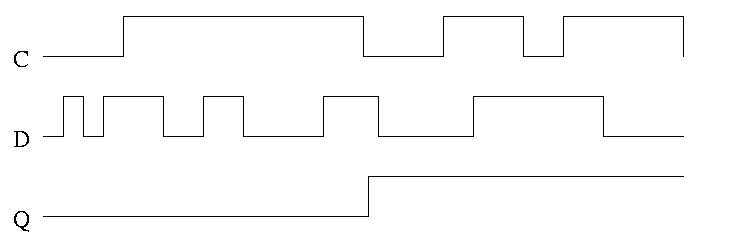
Note how much less wiggly the output is with the master-slave flop
than before with the transparent latch. As before we are assuming the
output is initially low.
Homework:
Try moving the inverter to the other latch
What has changed?
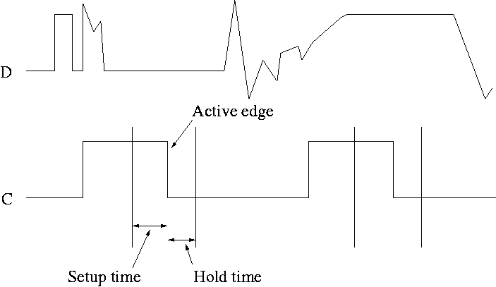
- This picture shows the setup and hold times discussed above.
- It is crucial when building circuits with flip flops that D is
stable during the interval between the setup and hold times.
- Note that D is wild outside the critical interval, but that is OK.
Homework:
B.18
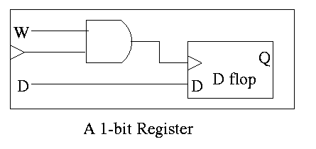
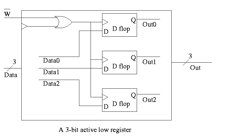
Registers
- Basically just an array of D flip-flops
- But what if you don't want to change the register during a
particular cycle?
- Introduce another input, the write line
- The write line is used to ``gate the clock''
- The book forgot the write line.
- Clearly if the write line is high forever, the clock input to
the register is passed right along to the D flop and hence the
input to the register is stored in the D flop when the active edge
occurs (for us the falling edge).
- Also clear is that if the write line is low forever, the clock
to the D flop is always low so has no edges and no writing occurs.
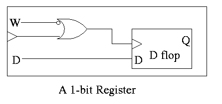
- But what about changing the write line?
- Assert or deassert the write line while the clock is low and
keep it at this value until the clock is low again.
- Not so good! Must have the write line correct quite a while
before the active edge. That is you must know whether you are
writing quite a while in advance.
- Better to do things so the write line must be correct when the
clock is high (i.e., just before the active edge
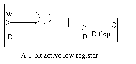
- An alternative is to use an active low write line,
i.e. have a W' input.
- Must have write line and data line valid during setup and hold
times
- To do a multibit register, just use multiple D flops.
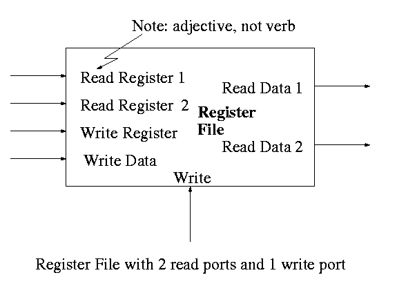
Register File
Set of registers each numbered
- Supply reg#, write line, and data (if a write)
- Can read and write same reg same cycle. You read the old value and
then the written value replaces this old value for subsequent cycles.
- Often have several read and write ports so that several
registers can be read and written during one cycle.
- We will do 2 read ports and one write port since that is
needed for ALU ops. This is Not adequate for superscalar (or
EPIC) or any other system where more than one operation is to be
calculated each cycle.
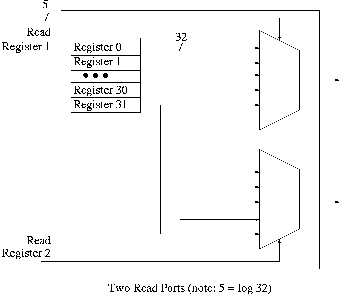
To read just need mux from register file to select correct
register.
- Have one of these for each read port
- Each is an n to 1 mux, b bits wide; where
- n is the number of registers (32 for MIPS)
- b is the width of each register (32 for MIPS)
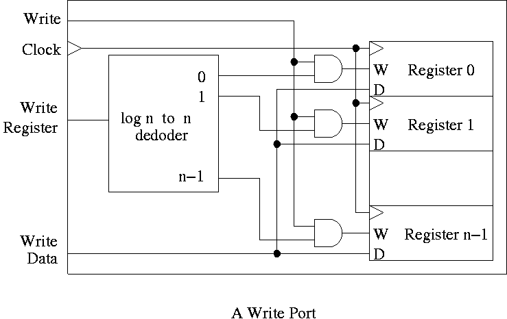
For writes use a decoder on register number to determine which
register to write. Note that 3 errors in the book's figure were fixed
- decoder is log n to n
- decoder outputs numbered 0 to n-1 (NOT n)
- clock is needed
The idea is to gate the write line with the output of the decoder. In
particular, we should perform a write to register r this cycle providing
- Recall that the inputs to a register are W, the write line, D the
data to write (if the write line is asserted) and the clock.
- The clock to each register is simply the clock input to the
register file.
- The data to each register is simply the write data to the register file.
- The write line to each register is unique
- The register number is fed to a decoder.
- The rth output of the decoder is asserted if r is the
specified register.
- Hence we wish to write register r if
- The write line to the register file is asserted
- The rth output of the decoder is asserted
- Bingo! We just need an and gate.
Homework: 20
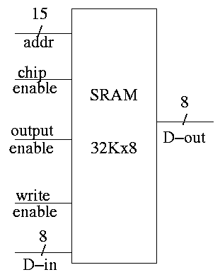
SRAMS and DRAMS
- External interface is on right
- 32Kx8 means it hold 32K words each 8 bits.
- Addr, D-in, and D-out are same as registers. Addr is 15
bits since 2 ^ 15 = 32K. D-out is 8 bits since we have a by 8
SRAM.
- Write enable is similar to the write line (unofficial: it
is a pulse; there is no clock),
- Output enable is for the three state (tri-state) drivers
discussed just below (unofficial).
- Ignore chip enable (perfer not to have all chips enabled
for electrical reasons).
- (Sadly) we will not look inside officially. Following is
unofficial
- Conceptually, an SRAM is like a register file but we can't
use the register file implementation for a large SRAM because
there would be too many wires and the muxes would be too big.
- Two stage decode.
- For a 32Kx8 SRAM would need a 15-32K decoder.
- Instead package the SRAM as eight 512x64 SRAMS.
- Pass 9 bits of the address through a 9-512 decoder and
use these 512 wires to select the appropriate 64-bit word
from each of the sub SRAMS. Use the remaining 6 bits to
select the appropriate bit from each 64-bit word.
- Tri-state buffers (drivers) used instead of a mux.
- I was fibbing when I said that signals always have a 1 or 0.
- However, we will not use tristate logic; we will use muxes.
- DRAM uses a version of the above two stage decode.
- View the memory as an array.
- First select (and save in a ``faster'' memory) an
entire row.
- Then select and output only one (or a few) column(s).
- So can speed up access to elts in same row.
- SRAM and ``logic'' are made from similar technologies but
DRAM technology is quite different.
- So easy to merge SRAM and CPU on one chip (SRAM
cache).
- Merging DRAM and CPU is more difficult but is now
being done.
- Error Correction (Omitted)
Note:
There are other kinds of flip-flops T, J-K. Also one could learn
about excitation tables for each. We will not cover this
material (H&P doesn't either). If interested, see Mano
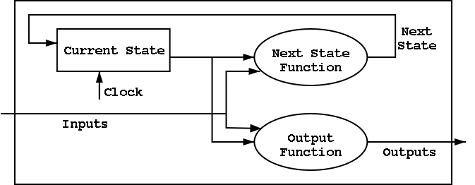
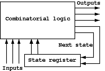
B.6: Finite State Machines
I do a different example from the book (counters instead of traffic
lights). The ideas are the same and the two generic pictures (below)
apply to both examples.
Counters
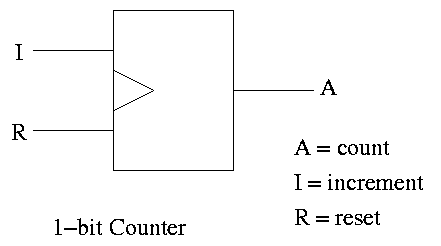
A counter counts (naturally).
- The counting is done in binary.
- Increments (i.e., counts) on clock ticks (active edge).
- Actually only on those clocks ticks when the ``increment'' line is
asserted.
- If reset asserted at a clock tick, the counter is reset to zero.
- What if both reset and increment assert?
Ans: Shouldn't do that. Will accept any answer (i.e., don't care).
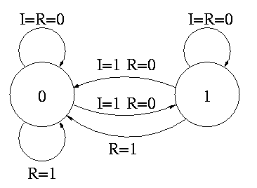
The state transition diagram
- The figure shows the state transition diagram for A, the output of
a 1-bit counter.
- In this implementation, if R=I=1 we choose to set A to zero. That
is, if Reset and Increment are both asserted, we do the Reset.
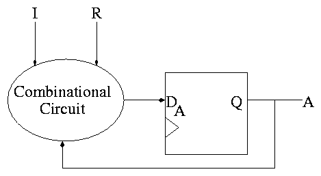
The circuit diagram.
- Uses one flop and a combinatorial circuit.
- The (combinatorial) circuit is determined by the transition diagram.
- The circuit must calculate the next value of A from the current
value and I and R.
- The flop producing A is often itself called A and the D input to this
flop is called DA (really D sub A).
How do we determine the combinatorial circuit?
- This circuit has three inputs, I, R, and the current A.
- It has one output, DA, which is the desired next A.
- So we draw a truth table, as before.
- For convenience I added the label Next A to the DA column
Current      || Next A
   A    I R  || DA <-- i.e. to what must I set DA
-------------++--      in order to get the desired
   0    0 0  || 0      Next A for the next cycle.
   1    0 0  || 1
   0    1 0  || 1
   1    1 0  || 0
   x    x 1  || 0
But this table is simply the truth table for the combinatorial
circuit.
A I R  || DA
-------++--
0 0 0  || 0
1 0 0  || 1
0 1 0  || 1
1 1 0  || 0
x x 1  || 0

DA = R' (A XOR I)
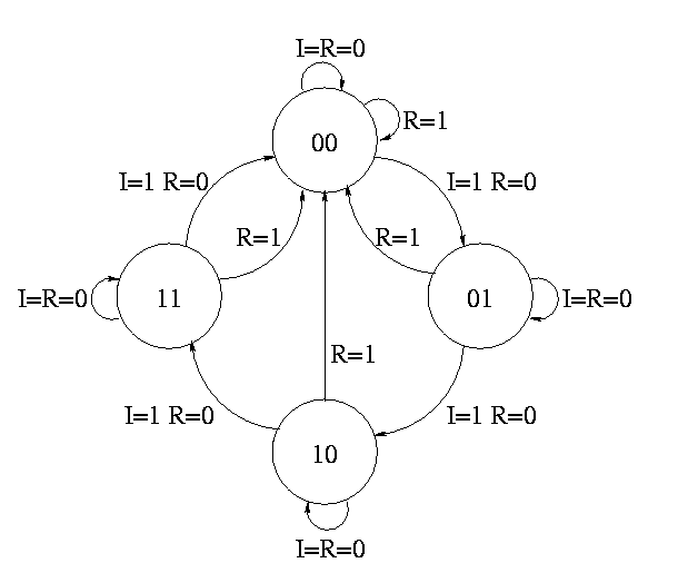
How about a two bit counter.
- State diagram has 4 states 00, 01, 10, 11 and transitions from one
to another
- The circuit diagram has 2 D flops
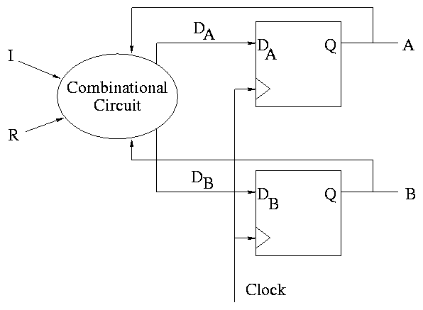
To determine the combinatorial circuit we could precede as before
Current      ||
  A B   I R  || DA DB
-------------++------
This would work but we can instead think about how a counter works and
see that.
DA = R'(A XOR I)
DB = R'(B XOR AI)
Homework: B.23
B.7 Timing Methodologies
Skipped
Allan Gottlieb