Computer Architecture
1999-2000 Fall
MW 3:30-4:45
Ciww 109
Allan Gottlieb
gottlieb@nyu.edu
http://allan.ultra.nyu.edu/~gottlieb
715 Broadway, Room 1001
212-998-3344
609-951-2707
email is best
======== START LECTURE #6
========

SRAMS and DRAMS
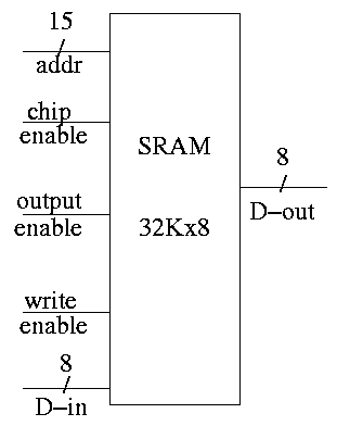
- External interface is on right
- 32Kx8 means it hold 32K words each 8 bits.
- Addr, D-in, and D-out are same as registers. Addr is 15
bits since 2 ^ 15 = 32K. D-out is 8 bits since we have a by 8
SRAM.
- Write enable is similar to the write line (unofficial: it
is a pulse; there is no clock),
- Output enable is for the three state (tri-state) drivers
discussed just below (unofficial).
- Ignore chip enable (perfer not to have all chips enabled
for electrical reasons).
- (Sadly) we will not look inside officially. Following is
unofficial
- Conceptually, an SRAM is like a register file but we can't
use the register file implementation for a large SRAM because
there would be too many wires and the muxes would be too big.
- Two stage decode.
- For a 32Kx8 SRAM would need a 15-32K decoder.
- Instead package the SRAM as eight 512x64 SRAMS.
- Pass 9 bits of the address through a 9-512 decoder and
use these 512 wires to select the appropriate 64-bit word
from each of the sub SRAMS. Use the remaining 6 bits to
select the appropriate bit from each 64-bit word.
- Tri-state buffers (drivers) used instead of a mux.
- I was fibbing when I said that signals always have a 1
or 0.
- However, we will not use tristate logic; we will use
muxes.
- DRAM uses a version of the above two stage decode.
- View the memory as an array.
- First select (and save in a ``faster'' memory) an
entire row.
- Then select and output only one (or a few) column(s).
- So can speed up access to elts in same row.
- SRAM and ``logic'' are made from similar technologies but
DRAM technology is quite different.
- So easy to merge SRAM and CPU on one chip (SRAM
cache).
- Merging DRAM and CPU is more difficult but is now
being done.
- Error Correction (Omitted)
Note:
There are other kinds of flip-flops T, J-K. Also one could learn
about excitation tables for each. We will not cover this
material (H&P doesn't either). If interested, see Mano
B.6: Finite State Machines
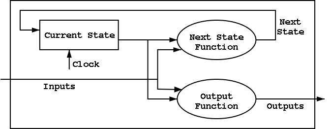
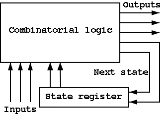
I do a different example from the book (counters instead of traffic
lights). The ideas are the same and the two generic pictures (below)
apply to both examples.


Counters

A counter counts (naturally).
- The counting is done in binary.
- Increments (i.e., counts) on clock ticks (active edge).
- Actually only on those clocks ticks when the ``increment'' line is
asserted.
- If reset asserted at a clock tick, the counter is reset to zero.
- What if both reset and increment assert?
Ans: Shouldn't do that. Will accept any answer (i.e., don't
care).

The state transition diagram
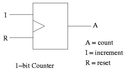
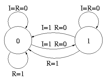
- The figure shows the state transition diagram for A, the output of
a 1-bit counter.
- In this implementation, if R=I=1 we choose to set A to zero. That
is, if Reset and Increment are both asserted, we do the Reset.

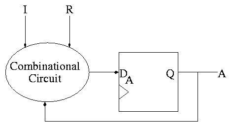
The circuit diagram.
- Uses one flop and a combinatorial circuit.
- The (combinatorial) circuit is determined by the transition
diagram.
- The circuit must calculate the next value of A from the current
value and I and R.
- The flop producing A is often itself called A and the D input to
this
flop is called DA (really D sub A).
How do we determine the combinatorial ciccuit?
- This circuit has three inputs, I, R, and the current A.
- It has one output, DA, which is the desired next A.
- So we draw a truth table, as before.
- For convenience I added the label Next A to the DA column
Current      || Next A
   A    I R  || DA <-- i.e. to what must I set DA
-------------++--      in order to get the desired
   0    0 0  || 0      Next A for the next cycle.
   1    0 0  || 1
   0    1 0  || 1
   1    1 0  || 0
   x    x 1  || 0
But this table is simply the truth table for the combinatorial
circuit.
A I R  || DA
-------++--
0 0 0  || 0
1 0 0  || 1
0 1 0  || 1
1 1 0  || 0
x x 1  || 0

DA = R' (A XOR I)
How about a two bit counter.
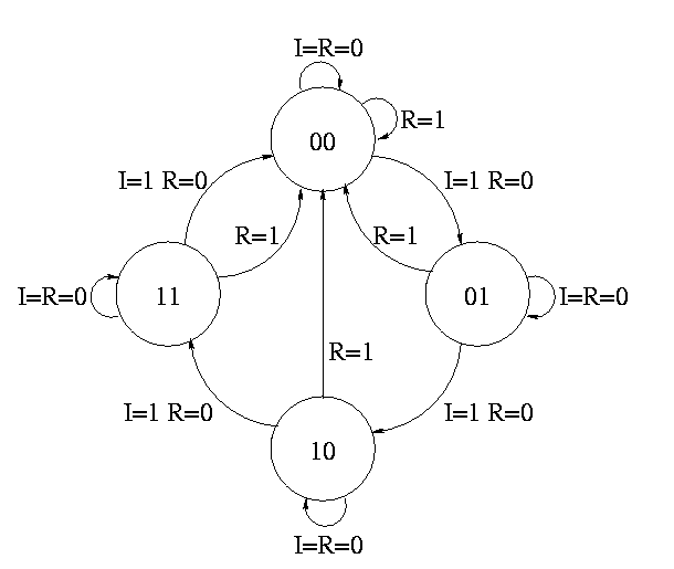
- State diagram has 4 states 00, 01, 10, 11 and transitions from one
to another
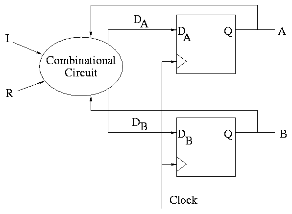
- The circuit diagram has 2 D flops


To determine the combinationatorial circuit we could preceed as before
Current      ||
  A B   I R  || DA DB
-------------++------
This would work but we can instead think about how a counter works and
see that.
DA = R'(A XOR I)
DB = R'(B XOR AI)
Homework: 23
B.7 Timing Methodologies
Skipped
Chapter 1
Homework:
READ chapter 1. Do 1.1 -- 1.26 (really one matching question)
Do 1.27 to 1.44 (another matching question),
1.45 (and do 7200 RPM and 10,000 RPM),
1.46, 1.50
Chapter 3
Homework:
Read sections 3.1 3.2 3.3
