Computer Architecture
1999-2000 Fall
MW 3:30-4:45
Ciww 109
Allan Gottlieb
gottlieb@nyu.edu
http://allan.ultra.nyu.edu/~gottlieb
715 Broadway, Room 1001
212-998-3344
609-951-2707
email is best
======== START LECTURE #4
========
Note:
I should have assigned B.5 as part of homework 2. I did include it in
the solutions. B.5 is the part for which the comment ``(Assume you
have constant signals 1 and 0 as well.)'' applies.
ROMs
One way to implement a mathematical (or C) function (without side
effects) is to perform a table lookup.
A ROM (Read Only Memory) is the analogous way to implement a logic
function.
- For a math function f we start with x and get f(x).
- For a ROM with start with the address and get the value stored at
that address.
- Normally math functions are defined for an infinite number of
values, for example f(x) = 3x for all real numbers x
- We can't build an infinite ROM (sorry), so we are only interested
in functions defined for a finite number of values. Today a million
is OK a billion is too big.
- How do we create a ROM for the function f(3)=4, f(6)=20 all other
values don't care?
Simply have the ROM store 4 in address 3 and 20 in address 6.
- Consider a function defined for all n-bit numbers (say n=20) and
having a k-bit output for each input.
- View an n-bit input as n 1-bit inputs.
- View a k-bit output as k 1-bit outputs.
- Since there are 2^n possible inputs and each requires a k 1-bit output,
there are a total of (2^n)k bits of output, i.e. the ROM must hold
(2^n)k bits.
- Now consider a truth table with n inputs and k outputs.
The total number of output bits is again (2^n)k (2^n rows and k output
columns).
- Thus the ROM implements a truth table, i.e. is a logic function.
Important: A ROM does not have state. It is
another combinational circuit. That is, it does not represent
``memory''. The reason is that once a ROM is manufactured, the output
depends only on the input.
A PROM
is a programmable ROM. That is you buy the ROM with ``nothing'' in
its memory and then before
it is placed in the circuit you load the memory, and never change it.
This is like a CD-R.
An EPROM is an erasable PROM. It costs more
but if you decide to change its memory this is possible (but is slow).
This is like a CD-RW.
``Normal'' EPROMs are erased by some ultraviolet light process. But
EEPROMs (electrically erasable PROMS) are faster and
are done electronically.
All these EPROMS are erasable not writable, i.e. you can't just change
one bit.
A ROM is similar to PLA
- Both can implement any truth table, in principle.
- A 2Mx8 ROM can really implment any truth table with 21 inputs
(2^21=2M) and 8 outputs.
- It stores 2M bytes
- In ROM-speak, it has 21 address pins and 8 data pins
- A PLA with 21 inputs and 8 outputs might need to have 2M minterms
(AND gates).
- The number of minterms depends on the truth table itself.
- For normal TTs with 21 inputs the number of minterms is MUCH
less than 2^21.
- The PLA is manufactured with the number of minterms needed
- Compare a PAL with a PROM
- Both can in principle implement any TT
- Both are user programmable
- A PROM with n inputs and k outputs can implement any TT with n
inputs and k outputs.
- A PAL that you buy does not have enough gates for all
possibilities since most TTs with n inputs and k outputs don't
require nearly (2^n)k gates.
Don't Cares
- Sometimes not all the input and output entries in a TT are
needed. We indicate this with an X and it can result in a smaller
truth table.
- Input don't cares.
- The output doesn't depend on all inputs, i.e. the output has
the same value no matter what value this input has.
- We saw this when we did muxes
- Output don't cares
- For some input values, either output is OK.
- This input combination is impossible.
- For this input combination, the given output is not used
(perhaps it is ``muxed out'' downstream)
Example (from the book):
- If A or C is true, then D is true (independent of B).
- If A or B is true, then E is true.
- F is true if exactly one of the inputs is true, but we don't care
about the value of F if both D and E are true
Full truth table
     A   B   C || D   E   F
     ----------++----------
     0   0   0 || 0   0   0
     0   0   1 || 1   0   1
     0   1   0 || 0   1   1
     0   1   1 || 1   1   0
     1   0   0 || 1   1   1
     1   0   1 || 1   1   0
     1   1   0 || 1   1   0
     1   1   1 || 1   1   1
This has 7 minterms.
Put in the output don't cares
     A   B   C || D   E   F
     ----------++----------
     0   0   0 || 0   0   0
     0   0   1 || 1   0   1
     0   1   0 || 0   1   1
     0   1   1 || 1   1   X
     1   0   0 || 1   1   X
     1   0   1 || 1   1   X
     1   1   0 || 1   1   X
     1   1   1 || 1   1   X
Now do the input don't cares
- B=C=1 ==> D=E=11 ==> F=X ==> A=X
- A=1 ==> D=E=11 ==> F=X ==> B=C=X
     A   B   C || D   E   F
     ----------++----------
     0   0   0 || 0   0   0
     0   0   1 || 1   0   1
     0   1   0 || 0   1   1
     X   1   1 || 1   1   X
     1   X   X || 1   1   X
These don't cares are important for logic minimization. Compare the
number of gates needed for the full TT and the reduced TT. There are
techniques for minimizing logic, but we will not cover them.
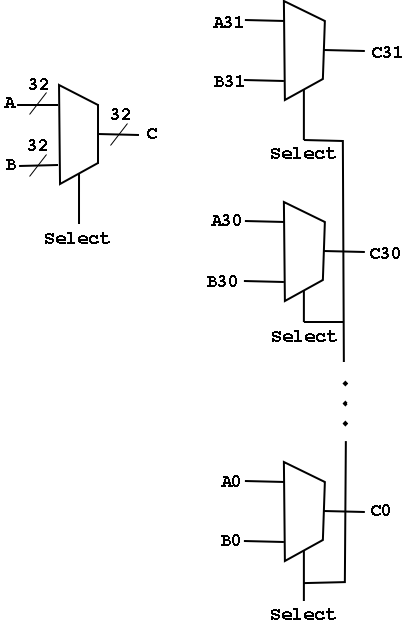
Arrays of Logic Elements
- Do the same thing to many signals
- Draw thicker lines and use the ``by n'' notation.
- Diagram below shows a 32-bit 2-way mux and an implementation with 32
1-bit, 2-way muxes.
- A Bus is a collection of data lines treated
as a single logical (n-bit) value.
- Use an array of logic elements to process a bus.
For example, the above mux switches between 2 32-bit buses.
*** Big Change Coming ***
Sequential Circuits, Memory, and State
Why do we want to have state?
- Memory (i.e. ram not just rom or prom)
- Counters
- Reducing gate count
- Multiplier would be quadradic in comb logic.
- With sequential logic (state) can do in linear.
- What follows is unofficial (i.e. too fast to
understand)
- Shift register holds partial sum
- Real slick is to share this shift reg with
multiplier
- We will do this circuit later in the course
Assume you have a real OR gate. Assume the two inputs are both
zero for an hour. At time t one input becomes 1. The output will
OSCILLATE for a while before settling on exactly 1. We want to be
sure we don't look at the answer before its ready.
B.4: Clocks
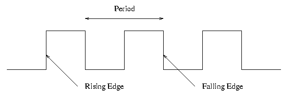
Frequency and period
- Hertz (Hz), Megahertz, Gigahertz vs. Seconds, Microseconds,
Nanoseconds
- Old (descriptive) name for Hz is cycles per second (CPS)
- Rate vs. Time
Edges
- Rising Edge; falling edge
- We use edge-triggered logic
- State changes occur only on a clock edge
- Will explain later what this really means
- One edge is called the Active edge
- The edge (rising or falling) on which changes occur
- Choice is technology dependent
- Sometimes trigger on both edges (e.g., RAMBUS or DDR memory)
Synchronous system
Now we are going to add state elements to the combinational
circuits we have been using previously.
Remember that a combinational/combinatorial circuits has its outpus
determined by its input, i.e. combinatorial circuits do not contain
state.
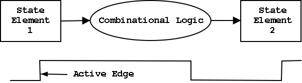
State elements include state (naturally).
- i.e., memory
- state-elements have clock as an input
- can change state only at active edge
- produce output Always; based on current state
- all signals that are written to state elements must be valid at
the time of the active edge.
- For example, if cycle time is 10ns make sure combinational circuit
used to compute new state values completes in 10ns
- So state elements change on active edge, comb circuit
stabilizes between active edges.
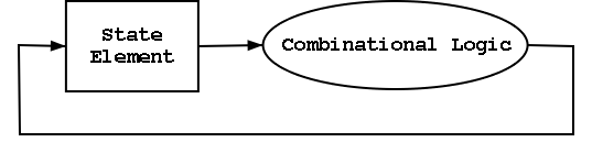
- Think of registers or memory as state elements.
- Can have loops like at the right.
- A loop like this is a cycle of the computer.
B.5: Memory Elements
We want edge-triggered clocked memory and will only use
edge-triggered clocked memory in our designs. However we get
there by stages. We first show how to build unclocked
memory; then using unclocked memory we build
level-sensitive clocked memory; finally from
level-sensitive clocked memory we build edge-triggered
clocked memory.
Unclocked Memory
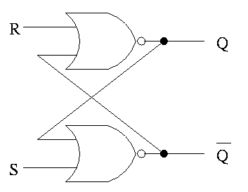
S-R latch (set-reset)
- ``Cross-coupled'' nor gates
- Don't assert both S and R at once
- When S is asserted (i.e., S=1 and R=0)
- the latch is Set (that's why it is called S)
- Q becomes true (Q is the output of the latch)
- Q' becomes false (Q' is the complemented output)
- When R is asserted
- the latch is Reset
- Q becomes false
- Q' becomes true
- When neither one is asserted
- The latch remains the same, i.e. Q and Q' stay as they
were
- This is the memory aspect
Clocked Memory: Flip-flops and latches
The S-R latch defined above is not clocked memory. Unfortunately the
terminology is not perfect.
For both flip-flops and
latches the output equals the value stored in the
structure. Both have an input and an output (and the complemented
output) and a clock input as well. The clock determines when the
internal value is set to the current input. For a latch, the change
occurs whenever the clock is asserted (level sensitive). For a
flip-flop, the change occurs at the active edge.
D latch
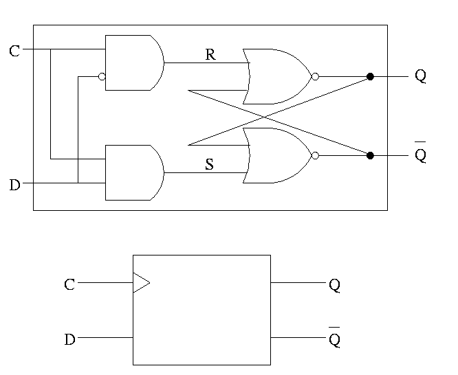
The D is for data
- The left part uses the clock.
- When the clock is low, both R and S are forced low.
- When the clock is high, S=D and R=D' so the value store is D.
- Output changes when input changes and the clock is asserted.
- Level sensitive rather than edge triggered.
- Sometimes called a transparent latch.
- We won't use these in designs.
- The right hand part of the circuit is the S-R (unclocked) latch we
just constructed.
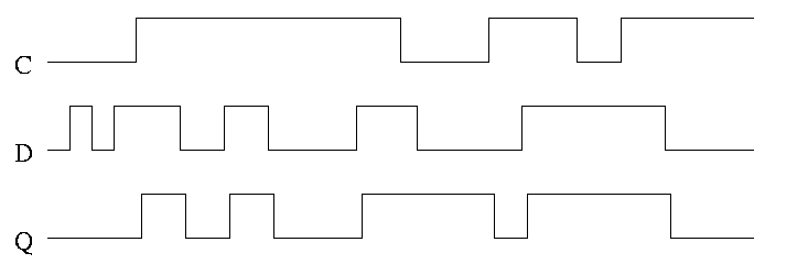
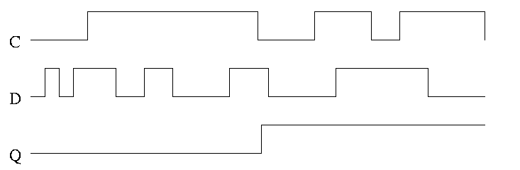
In the traces below notice how the output follows the input when the
clock is high and remains constant when the clock is low. We assume
the stored value is initially low.
D or Master-Slave Flip-flop
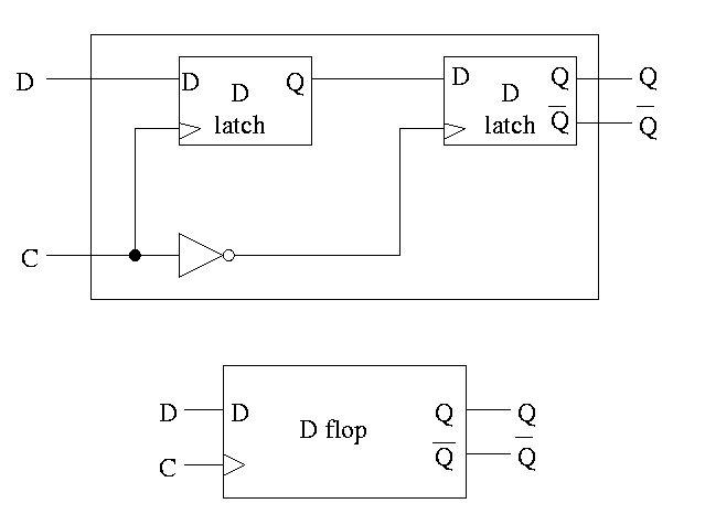
This was our goal. We now have an edge-triggered, clocked memory.
- Built from D latches, which are transparent
- The result is Not transparent
- Changes on the active edge
- This one has the falling edge as active edge
- Sometimes called a master-slave flip-flop
- Note substructures with letters reused
having different meaning (block structure a la algol)
- Master latch (the left one) is set during the time clock is
asserted.
Remember that the latch is transparent, i.e. follows
its input when its clock is asserted. But the second
latch is ignoring its input at this time. When the
clock falls, the 2nd latch pays attention and the
first latch keeps producing whatever D was at
fall-time.
- Actually D must remain constant for some time around
the active edge.
- The set-up time before the edge
- The hold time after the edge
- See diagram below
Note how much less wiggly the output is with the master-slave flop
than before with the transparent latch. As before we are assuming the
output is initially low.
Homework:
Try moving the inverter to the other latch
What has changed?