Computer Architecture
1999-2000 Fall
MW 3:30-4:45
Ciww 109
Allan Gottlieb
gottlieb@nyu.edu
http://allan.ultra.nyu.edu/~gottlieb
715 Broadway, Room 1001
212-998-3344
609-951-2707
email is best
======== START LECTURE #3
========
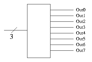
Decoder
- Note the ``3'' with a slash, which signifies a three bit input.
This notation represents three (1-bit) wires.
- A decoder with n input bits, produces 2^n output bits.
- View the input as ``k written an n-bit binary number'' and
view the output as 2^n bits with the k-th bit set and all the
other bits clear.
- Implement on board with AND/OR.
- Why do we use decoders and encoders?
- The encoded form takes (MANY) fewer bits so is better for
communication.
- The decoded form is easier to work with in hardware since
there is no direct way to test if 8 wires represent a 5
(101). You would have to test each wire. But it easy to see
if the encoded form is a five (00100000)
Encoder
- Reverse "function" of decoder.
- Not defined for all inputs (exactly one must be 1)
Sneaky way to see that NAND is universal.
- First show that you can get NOT from NAND. Hence we can build
inverters.
- Now imagine that you are asked to do a circuit for some function
with N inputs. Assume you have only one output.
- Using inverters you can get 2N signals the N original and N
complemented.
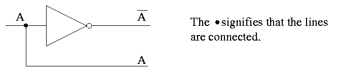
- Recall that the natural sum of products form is a bunch of ORs
feeding into one AND.
- Naturally you can add pairs of bubbles since they ``cancel''
- But these are all NANDS!!
Half Adder
- Two 1-bit inputs: X and Y
- Two 1-bit outputs S and Co (carry out)
- No carry in
- Draw TT
Homework: Draw logic diagram
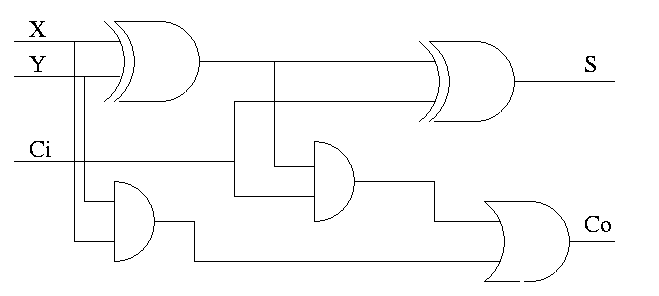
Full Adder
- Three 1-bit inputs: X, Y and Ci.
- Two 1-bit output: S and Co
- S = ``the total number of 1s in X, Y, and Ci is odd''
- Co = #1s is at least 2
Homework:
- Draw TT (8 rows)
- Show S = X XOR Y XOR Ci
- Show Co = XY + (X XOR Y)Ci
How about 4 bit adder ?
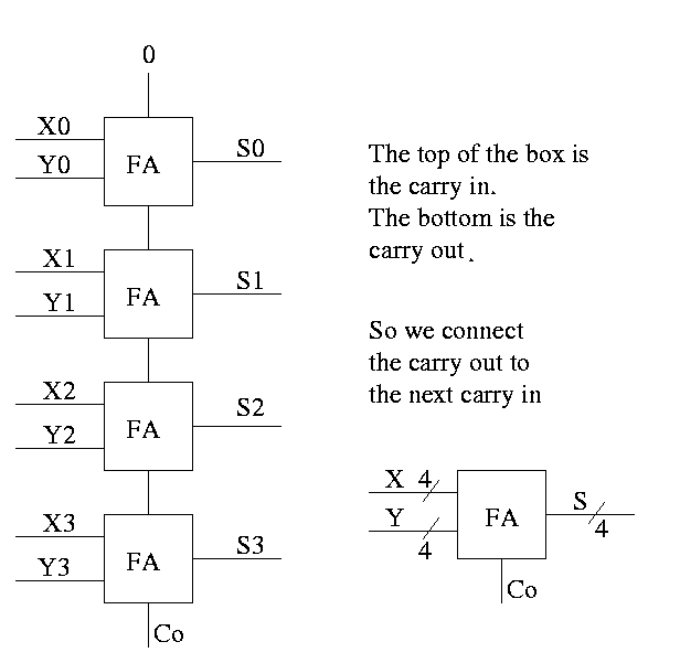
How about an n-bit adder ?
- Linear complexity, i.e. the time for a 64-bit add is twice
that for a 32-bit add.
- Called ripple carry since the carry ripples down the circuit
from the low order bit to the high order bit. This is why the
circuit has linear complexity.
- Faster methods exist. Indeed we will learn one soon.
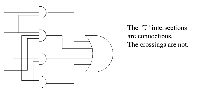
PLAs--Programmable Logic Arrays
Idea is to make use of the algorithmic way you can look at a TT and
produce a circuit diagram in the sums of product form.
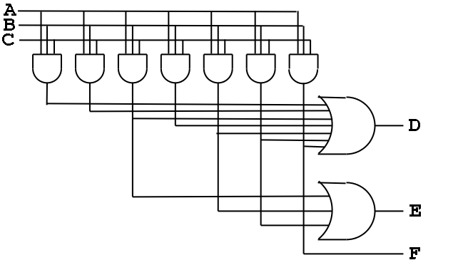
Consider the following TT from the book (page B-13)
     A | B | C || D | E | F
     --+---+---++---+---+--
     O | 0 | 0 || 0 | 0 | 0
     0 | 0 | 1 || 1 | 0 | 0
     0 | 1 | 0 || 1 | 0 | 0
     0 | 1 | 1 || 1 | 1 | 0
     1 | 0 | 0 || 1 | 0 | 0
     1 | 0 | 1 || 1 | 1 | 0
     1 | 1 | 0 || 1 | 1 | 0
     1 | 1 | 1 || 1 | 0 | 1
- Recall how we construct a circuit from a truth table.
- The circuit is in sum of products form.
- There is a big OR for each output. The OR has one
input for each row that the output is true.
- Since there are 7 rows for which at least one output is true,
there are 7 product terms that will be used in one
or more of the ORs (in fact all seven will be used in D, but that is
special to this example)
- Each of these product terms is called a Minterm
- So we need a bunch of ANDs (in fact, seven, one for each minterm)
taking A, B, C, A', B', and C' as inputs.
- This is called the AND plane and the collection of
ORs mentioned above is called the OR plane.
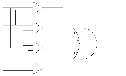
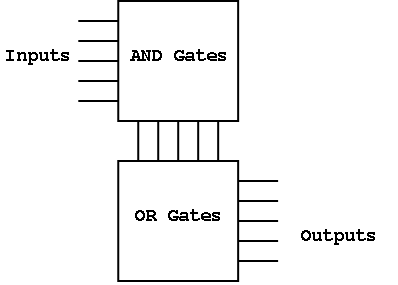
Here is the circuit diagram for this truth table.
Here it is redrawn in a more schmatic style.
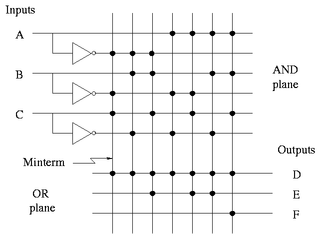
- This figure shows more clearly the AND plane, the OR plane, and
the minterms.
- Rather than having bubbles (i.e., custom AND gates that invert
certain inputs), we
simply invert each input once and send the inverted signal all the way
accross.
- AND gates are shown as vertical lines; ORs as horizontal.
- Note the dots to represent connections.
- Imagine building a bunch of these but not yet specifying where the
dots go. This would be a generic precurson to a PLA.
Finally, it can be redrawn in a more abstract form.
Before a PLA is manufactured all the connections are specified.
That is, a PLA is specific for a given circuit. It is somewhat of a
misnomer since it is notprogrammable by the user
Homework: B.10 and B.11
Can also have a PAL or Programmable array logic
in which the final dots are specified
by the user. The manufacturer produces a ``sea of gates''; the user
programs it to the desired logic function by adding the dots.