Computer Architecture
1999-2000 Fall
MW 3:30-4:45
Ciww 109
Allan Gottlieb
gottlieb@nyu.edu
http://allan.ultra.nyu.edu/~gottlieb
715 Broadway, Room 1001
212-998-3344
609-951-2707
email is best
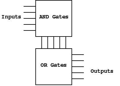
0: Administrivia
Web Pages
There is a web page for the course. You can find it from my home
page, which is http://allan.ultra.nyu.edu/~gottlieb
- I will soon mirror my home page on the CS web site
- You can find these notes there on the course home page.
Please let me know if you can't find it.
- The notes will be updated as bugs are found.
- I will also produce a separate page for each lecture after the
lecture is given. These individual pages
might not get updated as quickly as the large page
Textbook
Text is Hennessy and Patterson ``Computer Organization and Design
The Hardware/Software Interface'', 2nd edition.
- Available in the bookstore.
- Used last year so probably used copies exist
- The main body of the book assumes you know logic design.
- I do NOT make that assumption.
- We will start with appendix B, which is logic design review.
- A more extensive treatment of logic design is M. Morris Mano
``Computer System Architecture'', Prentice Hall.
- We will not need as much as Mano covers and it is not a cheap book so
I am not requiring you to get it. I will have it put into the library.
- My treatment will follow H&P not mano.
- Most of the figures in these notes are based on figures from the
course textbook. The following copyright notice applies.
``All figures from Computer Organization and Design:
The Hardware/Software Approach, Second Edition, by
David Patterson and John Hennessy, are copyrighted
material (COPYRIGHT 1998 MORGAN KAUFMANN
PUBLISHERS, INC. ALL RIGHTS RESERVED).
Figures may be reproduced only for classroom or
personal educational use in conjunction with the book
and only when the above copyright line is included. They
may not be otherwise reproduced, distributed, or
incorporated into other works without the prior written
consent of the publisher.''
Computer Accounts and mailman mailing list
- You are entitled to a computer account, get it.
- Sign up for the course mailman mailing list.
http://www.cs.nyu.edu/mailman/listinfo/v22_0436_001_fl00
- If you want to send mail to me, use gottlieb@nyu.edu not
the mailing list.
- You may do assignments on any system you wish, but ...
- You are responsible for the machine. I extend deadlines if
the nyu machines are down, not if yours is.
- Be sure to upload your assignments to the
nyu systems.
- If somehow your assignment is misplaced by me or a grader,
we need a to have a copy ON AN NYU SYSTEM
that can be used to verify the date the lab was completed.
- When you complete a lab (and have it on an nyu system), do
not edit those files. Indeed, put the lab in a separate
directory and keep out of the directory. You do not want to
alter the dates.
Homeworks and Labs
I make a distinction between homework and labs.
Labs are
- Required
- Due several lectures later (date given on assignment)
- Graded and form part of your final grade
- Penalized for lateness
Homeworks are
- Optional
- Due beginning of Next lecture
- Not accepted late
- Mostly from the book
- Collected and returned
- Can help, but not hurt, your grade
Upper left board for assignments and announcements
Appendix B: Logic Design
Homework: Read B1
B.2: Gates, Truth Tables and Logic Equations
Homework: Read B2
Digital ==> Discrete
Primarily (but NOT exclusively) binary at the hardware level
Use only two voltages--high and low.
- This hides a great deal of engineering.
- Must make sure not to sample the signal when not in one of these two states.
- Sometimes it is just a matter of waiting long enough
(determines the clock rate i.e. how many megahertz).
- Other times it is worse and you must avoid glitches.
- Oscilloscope traces shown below.
- Vertical axis is voltage; horizontal axis is time.
- Square wave--the ideal. How we think of circuits
- (Poorly drawn) Sine wave
- Actual wave
- Non-zero rise times and fall times
- Overshoots and undershoots
- Glitches
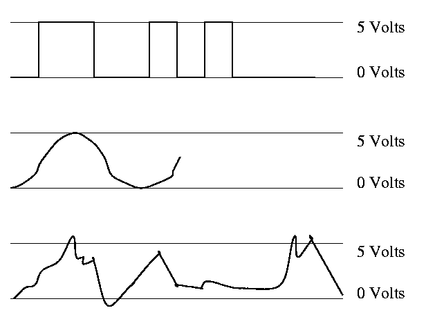
Since this is not an engineering course, we will ignore these
issues and assume square waves.
In English digital implies 10 (based on digit, i.e. finger),
but not in computers.
Bit = Binary digIT
Instead of saying high voltage and low voltage, we say true and false
or 1 and 0 or asserted and deasserted.
0 and 1 are called complements of each other.
A logic block can be thought of as a black box that takes signals in
and produces signals out. There are two kinds of blocks
- Combinational (or combinatorial)
- Does NOT have memory elements.
- Is simpler than circuits with memory since the outputs are a
function of the inputs. That is, if the same inputs are presented on
Monday and Tuesday, the same outputs will result.
- Sequential
- Contains memory.
- The current value in the memory is called the state of the block.
- The output depends on the input AND the state.
We are doing combinational blocks now. Will do sequential blocks
later (in a few lectures).
TRUTH TABLES
Since combinatorial logic has no memory, it is simply a function from
its inputs to its outputs. A
Truth Table has as columns all inputs
and all outputs. It has one row for each possible set of input values
and the output columns have the output for that input. Let's start
with a really simple case a logic block with one input and one output.
There are two columns (1 + 1) and two rows (2**1).
In  Out
0   ?
1   ?
How many are there?
How many different truth tables are there for a ``one in one out''
logic block?
Just 4: The constant functions 1 and 0, the identity, and an inverter
(pictures in a few minutes). There were two `?'s in the above table
each can be a 0 or 1 so 2**2 possibilities.
OK. Now how about two inputs and 1 output.
Three columns (2+1) and 4 rows (2**2).
In1 In2  Out
0   0    ?
0   1    ?
1   0    ?
1   1    ?
How many are there? It is just the number ways can you fill in the
output entries, i.e. the question marks. There are 4 output entries
so answer is 2**4=16.
How about 2 in and 8 out?
- 10 cols
- 4 rows
- 2**(4*8)=4 billion possible
3 in and 8 out?
- 11 cols
- 8 rows
- 2**(8**8)=2**64 possible
n in and k out?
- n+k cols
- 2**n rows
- 2**([2**n]*k) possible
Gets big fast!
Boolean algebra
Certain logic functions (i.e. truth tables) are quite common and
familiar.
We use a notation that looks like algebra to express logic functions and
expressions involving them.
The notation is called Boolean algebra in honor of
George Boole.
A Boolean value is a 1 or a 0.
A Boolean variable takes on Boolean values.
A Boolean function takes in boolean variables and produces boolean values.
- The (inclusive) OR Boolean function of two variables. Draw its
truth table. This is written + (e.g. X+Y where X and Y are Boolean
variables) and often called the logical sum. (Three out of four
output values in the truth table look right!)
- AND. Draw TT. Called logical product and written as a centered dot
(like product in regular algebra). All four values look right.
- NOT. Draw TT. This is a unary operator (One argument, not two
as above; functions with two inputs are called binary). Written A with a bar
over it. I will use ' instead of a bar as it is easier for me to type
in html.
- Exclusive OR (XOR). Written as + with a circle around it. True if
exactly one input is true (i.e., true XOR true = false). Draw TT.
Homework:
Consider the Boolean function of 3 boolean variables that is true
if and only if exactly 1 of the three variables is true. Draw the TT.
Some manipulation laws. Remember this is Boolean ALGEBRA.
Identity:
-
A+0 = 0+A = A
-
A.1 = 1.A = A
-
(using . for and)
Inverse:
- A+A' = A'+A = 1
- A.A' = A'.A = 0
- (using ' for not)
Both + and . are commutative so my identity and inverse examples
contained redundancy.
The name inverse law is somewhat funny since you
Add the inverse and get the identity for Product
or Multiply by the inverse and get the identity for Sum.
Associative:
- A+(B+C) = (A+B)+C
- A.(B.C)=(A.B).C
Due to the associative law we can write A.B.C since either order of
evaluation gives the same answer. Similarly we can write A+B+C.
We often elide the . so the product associative law is A(BC)=(AB)C.
So we better not have three variables A, B, and AB. In fact, we
normally use one letter variables.
Distributive:
- A(B+C)=AB+AC
- A+(BC)=(A+B)(A+C)
- Note that BOTH distributive laws hold UNLIKE ordinary arithmetic.
How does one prove these laws??
- Simple (but long). Write the TTs for each and see that the outputs
are the same.
- Prove the first distributive laws on the board.
Homework: Prove the second distributive law.
Let's do (on the board) the examples on pages B-5 and B-6.
Consider a logic function with three inputs A, B, and C; and three
outputs D, E, and F defined as follows: D is true if at least one
input is true, E if exactly two are true, and F if all three are true.
(Note that by ``if'' we mean ``if and only if''.
Draw the truth table.
Show the logic equations.
- For E first use the obvious method of writing one condition
for each 1-value in the E column i.e.
(A'BC) + (AB'C) + (ABC')
- Observe that E is true if two (but not three) inputs are true,
i.e.,
(AB+AC+BC) (ABC)' (using . higher precedence than +)
The first way we solved part E shows that any logic function
can be written using just AND, OR, and NOT. Indeed, it is in a nice
form. Called two levels of logic, i.e. it is a sum of products of
just inputs and their compliments.
DeMorgan's laws:
- (A+B)' = A'B'
- (AB)' = A'+B'
You prove DM laws with TTs. Indeed that is ...
Homework: B.6 on page B-45.
Do beginning of HW on the board.
======== START LECTURE #2
========
With DM (DeMorgan's Laws) we can do quite a bit without resorting to
TTs. For example one can show that the two expressions for E in the
example above (page B-6) are equal. Indeed that is
Homework: B.7 on page B-45
Do beginning of HW on board.
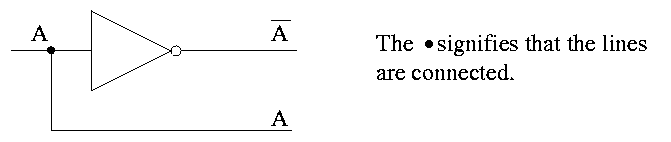
GATES
Gates implement basic logic functions: AND OR NOT XOR Equivalence
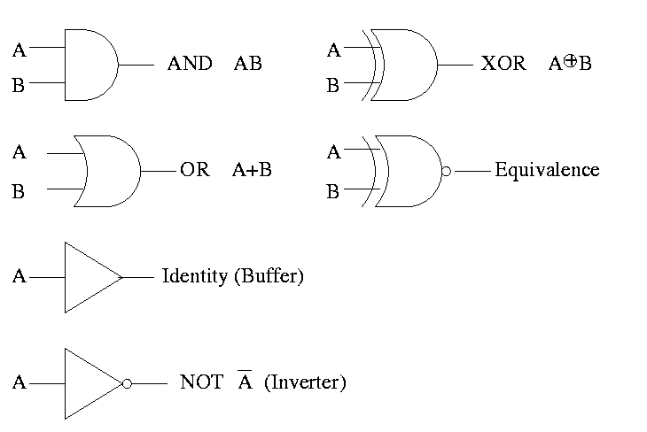
Often omit the inverters and draw the little circles at the input or
output of the other gates (AND OR). These little circles are
sometimes called bubbles.
This explains why the inverter is drawn as a buffer with a bubble.
Show why the picture for equivalence is the negation of XOR, i.e (A
XOR B)' is AB + A'B'
(A XOR B)' =
(A'B+AB')' =
(A'B)' (AB')' =
(A''+B') (A'+B'') =
(A + B') (A' + B) =
AA' + AB + B'A' + B'B =
0   + AB + B'A' + 0 =
AB + A'B'
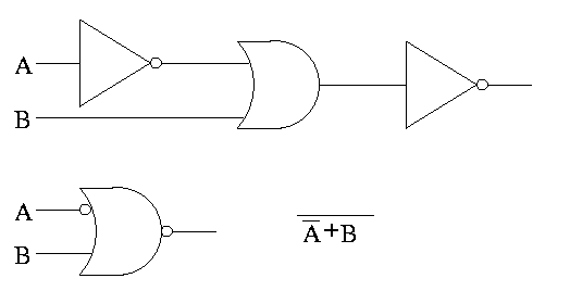
Homework: B.2 on page B-45 (I previously did the first part
of this homework).
Homework: Consider the Boolean function of 3 boolean vars
(i.e. a three input function) that is true if and only if exactly 1 of
the three variables is true. Draw the TT. Draw the logic diagram
with AND OR NOT. Draw the logic diagram with AND OR and bubbles.
A set of gates is called universal if these gates are
sufficient to generate all logic functions.
-
We have seen that any logic function can be constructed from AND OR
NOT. So this triple is universal.
-
Are there any pairs that are universal?
Ans: Sure, A+B = (A'B')' so can get OR from AND and NOT. Hence the
pair AND NOT is universal
Similarly, can get AND from OR and NOT and hence the pair OR NOT
is universal
-
Could there possibly be a single function that is universal all by
itself?
AND won't work as you can't get NOT from just AND
OR won't work as you can't get NOT from just OR
NOT won't work as you can't get AND from just NOT.
-
But there indeed is a universal function! In fact there are two.
NOR (NOT OR) is true when OR is false. Do TT.
NAND (NOT AND) is true when AND is false. Do TT.
Draw two logic diagrams for each, one from the definition and an
equivalent one with bubbles.
Theorem
A 2-input NOR is universal and
a 2-input NAND is universal.
Proof
We must show that you can get A', A+B, and AB using just a two input
NOR.
- A' = A NOR A
- A+B = (A NOR B)' (we can use ' by above)
- AB = (A' OR B')'
Homework: Show that a 2-input NAND is universal.
Can draw NAND and NOR each two ways (because (AB)' = A' + B')
We have seen how to get a logic function from a TT. Indeed we can
get one that is just two levels of logic. But it might not be the
simplest possible. That is, we may have more gates than are necessary.
Trying to minimize the number of gates is NOT trivial. Mano covers
the topic of gate minimization in detail. We will not cover it in
this course. It is not in H&P. I actually like it but must admit
that it takes a few lectures to cover well and it not used much in
practice since it is algorithmic and is done automatically by CAD
tools.
Minimization is not unique, i.e. there can be two or more minimal
forms.
Given A'BC + ABC + ABC'
Combine first two to get BC + ABC'
Combine last two to get A'BC + AB
Sometimes when building a circuit, you don't care what the output is
for certain input values. For example, that input combination might
be known not to occur. Another example occurs when, for some
combination of input values, a later part of the circuit will ignore
the output of this part. These are called don't care
outputs situations. Making use of don't cares can reduce the
number of gates needed.
Can also have don't care inputs
when, for certain values of a subset of the inputs, the output is
already determined and you don't have to look at the remaining
inputs. We will see a case of this in the very next topic, multiplexors.
An aside on theory
Putting a circuit in disjunctive normal form (i.e. two levels of
logic) means that every path from the input to the output goes through
very few gates. In fact only two, an OR and an AND. Maybe we should
say three since the AND can have a NOT (bubble). Theorticians call
this number (2 or 3 in our case) the depth of the circuit.
Se we see that every logic function can be implemented with small
depth. But what about the width, i.e., the number of gates.
The news is bad. The parity function takes n inputs
and gives TRUE if and only if the number of TRUE inputs is odd.
If the depth is fixed (say limited to 3), the number of gates needed
for parity is exponential in n.
B.3 COMBINATIONAL LOGIC
Homework:
Read B.3.
Generic Homework:
Read sections in book corresponding to the lectures.
Multiplexor
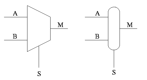
Often called a mux or a selector
Show equiv circuit with AND OR
Hardware if-then-else
    if S=0
        M=A
    else
        M=B
    endif
Can have 4 way mux (2 selector lines)
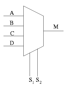
This is an if-then-elif-elif-else
   if S1=0 and S2=0
        M=A
    elif S1=0 and S2=1
        M=B
    elif S1=1 and S2=0
        M=C
    else -- S1=1 and S2=1
        M=D
    endif
Do a TT for 2 way mux. Redo it with don't care values.
Do a TT for 4 way mux with don't care values.
Homework:
B.12.
B.5 (Assume you have constant signals 1 and 0 as well.)
======== START LECTURE #3
========
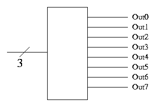
Decoder
- Note the ``3'' with a slash, which signifies a three bit input.
This notation represents three (1-bit) wires.
- A decoder with n input bits, produces 2^n output bits.
- View the input as ``k written an n-bit binary number'' and
view the output as 2^n bits with the k-th bit set and all the
other bits clear.
- Implement on board with AND/OR.
- Why do we use decoders and encoders?
- The encoded form takes (MANY) fewer bits so is better for
communication.
- The decoded form is easier to work with in hardware since
there is no direct way to test if 8 wires represent a 5
(101). You would have to test each wire. But it easy to see
if the encoded form is a five (00100000)
Encoder
- Reverse "function" of decoder.
- Not defined for all inputs (exactly one must be 1)
Sneaky way to see that NAND is universal.
- First show that you can get NOT from NAND. Hence we can build
inverters.
- Now imagine that you are asked to do a circuit for some function
with N inputs. Assume you have only one output.
- Using inverters you can get 2N signals the N original and N
complemented.
- Recall that the natural sum of products form is a bunch of ORs
feeding into one AND.
- Naturally you can add pairs of bubbles since they ``cancel''
- But these are all NANDS!!
Half Adder
- Two 1-bit inputs: X and Y
- Two 1-bit outputs S and Co (carry out)
- No carry in
- Draw TT
Homework: Draw logic diagram
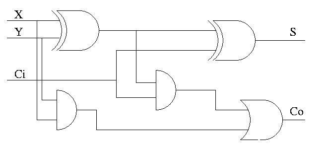
Full Adder
- Three 1-bit inputs: X, Y and Ci.
- Two 1-bit output: S and Co
- S = ``the total number of 1s in X, Y, and Ci is odd''
- Co = #1s is at least 2
Homework:
- Draw TT (8 rows)
- Show S = X XOR Y XOR Ci
- Show Co = XY + (X XOR Y)Ci
How about 4 bit adder ?
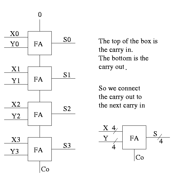
How about an n-bit adder ?
- Linear complexity, i.e. the time for a 64-bit add is twice
that for a 32-bit add.
- Called ripple carry since the carry ripples down the circuit
from the low order bit to the high order bit. This is why the
circuit has linear complexity.
- Faster methods exist. Indeed we will learn one soon.
PLAs--Programmable Logic Arrays
Idea is to make use of the algorithmic way you can look at a TT and
produce a circuit diagram in the sums of product form.
Consider the following TT from the book (page B-13)
     A | B | C || D | E | F
     --+---+---++---+---+--
     O | 0 | 0 || 0 | 0 | 0
     0 | 0 | 1 || 1 | 0 | 0
     0 | 1 | 0 || 1 | 0 | 0
     0 | 1 | 1 || 1 | 1 | 0
     1 | 0 | 0 || 1 | 0 | 0
     1 | 0 | 1 || 1 | 1 | 0
     1 | 1 | 0 || 1 | 1 | 0
     1 | 1 | 1 || 1 | 0 | 1
- Recall how we construct a circuit from a truth table.
- The circuit is in sum of products form.
- There is a big OR for each output. The OR has one
input for each row that the output is true.
- Since there are 7 rows for which at least one output is true,
there are 7 product terms that will be used in one
or more of the ORs (in fact all seven will be used in D, but that is
special to this example)
- Each of these product terms is called a Minterm
- So we need a bunch of ANDs (in fact, seven, one for each minterm)
taking A, B, C, A', B', and C' as inputs.
- This is called the AND plane and the collection of
ORs mentioned above is called the OR plane.
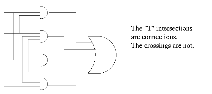
Here is the circuit diagram for this truth table.
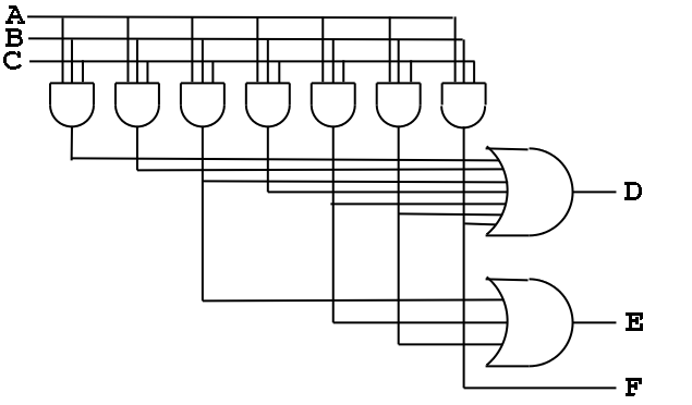
Here it is redrawn in a more schmatic style.
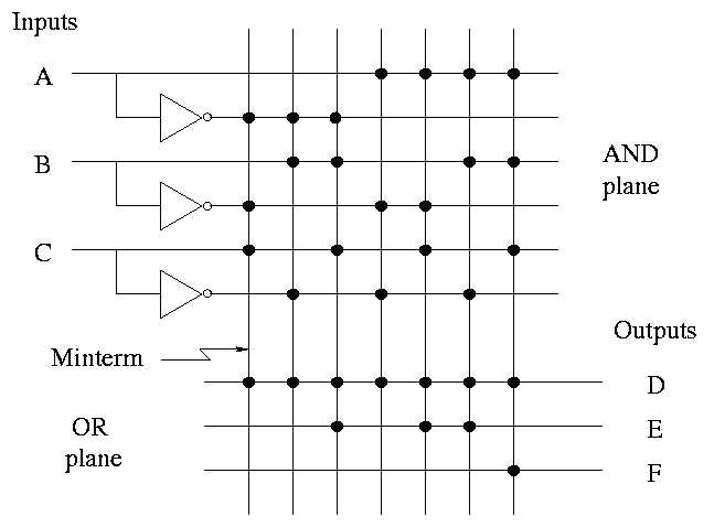
- This figure shows more clearly the AND plane, the OR plane, and
the minterms.
- Rather than having bubbles (i.e., custom AND gates that invert
certain inputs), we
simply invert each input once and send the inverted signal all the way
accross.
- AND gates are shown as vertical lines; ORs as horizontal.
- Note the dots to represent connections.
- Imagine building a bunch of these but not yet specifying where the
dots go. This would be a generic precurson to a PLA.
Finally, it can be redrawn in a more abstract form.
Before a PLA is manufactured all the connections are specified.
That is, a PLA is specific for a given circuit. It is somewhat of a
misnomer since it is notprogrammable by the user
Homework: B.10 and B.11
Can also have a PAL or Programmable array logic
in which the final dots are specified
by the user. The manufacturer produces a ``sea of gates''; the user
programs it to the desired logic function by adding the dots.
======== START LECTURE #4
========
ROMs
One way to implement a mathematical (or C) function (without side
effects) is to perform a table lookup.
A ROM (Read Only Memory) is the analogous way to implement a logic
function.
- For a math function f we start with x and get f(x).
- For a ROM with start with the address and get the value stored at
that address.
- Normally math functions are defined for an infinite number of
values, for example f(x) = 3x for all real numbers x
- We can't build an infinite ROM (sorry), so we are only interested
in functions defined for a finite number of values. Today a million
is OK a billion is too big.
- How do we create a ROM for the function f(3)=4, f(6)=20 all other
values don't care?
Simply have the ROM store 4 in address 3 and 20 in address 6.
- Consider a function defined for all n-bit numbers (say n=20) and
having a k-bit output for each input.
- View an n-bit input as n 1-bit inputs.
- View a k-bit output as k 1-bit outputs.
- Since there are 2^n possible inputs and each requires a k 1-bit output,
there are a total of (2^n)k bits of output, i.e. the ROM must hold
(2^n)k bits.
- Now consider a truth table with n inputs and k outputs.
The total number of output bits is again (2^n)k (2^n rows and k output
columns).
- Thus the ROM implements a truth table, i.e. is a logic function.
Important: A ROM does not have state. It is
another combinational circuit. That is, it does not represent
``memory''. The reason is that once a ROM is manufactured, the output
depends only on the input.
A PROM
is a programmable ROM. That is you buy the ROM with ``nothing'' in
its memory and then before
it is placed in the circuit you load the memory, and never change it.
This is like a CD-R.
An EPROM is an erasable PROM. It costs more
but if you decide to change its memory this is possible (but is slow).
This is like a CD-RW.
``Normal'' EPROMs are erased by some ultraviolet light process. But
EEPROMs (electrically erasable PROMS) are faster and
are done electronically.
All these EPROMS are erasable not writable, i.e. you can't just change
one bit.
A ROM is similar to PLA
- Both can implement any truth table, in principle.
- A 2Mx8 ROM can really implment any truth table with 21 inputs
(2^21=2M) and 8 outputs.
- It stores 2M bytes
- In ROM-speak, it has 21 address pins and 8 data pins
- A PLA with 21 inputs and 8 outputs might need to have 2M minterms
(AND gates).
- The number of minterms depends on the truth table itself.
- For normal TTs with 21 inputs the number of minterms is MUCH
less than 2^21.
- The PLA is manufactured with the number of minterms needed
- Compare a PAL with a PROM
- Both can in principle implement any TT
- Both are user programmable
- A PROM with n inputs and k outputs can implement any TT with n
inputs and k outputs.
- A PAL that you buy does not have enough gates for all
possibilities since most TTs with n inputs and k outputs don't
require nearly (2^n)k gates.
Don't Cares
- Sometimes not all the input and output entries in a TT are
needed. We indicate this with an X and it can result in a smaller
truth table.
- Input don't cares.
- The output doesn't depend on all inputs, i.e. the output has
the same value no matter what value this input has.
- We saw this when we did muxes
- Output don't cares
- For some input values, either output is OK.
- This input combination is impossible.
- For this input combination, the given output is not used
(perhaps it is ``muxed out'' downstream)
Example (from the book):
- If A or C is true, then D is true (independent of B).
- If A or B is true, then E is true.
- F is true if exactly one of the inputs is true, but we don't care
about the value of F if both D and E are true
Full truth table
     A   B   C || D   E   F
     ----------++----------
     0   0   0 || 0   0   0
     0   0   1 || 1   0   1
     0   1   0 || 0   1   1
     0   1   1 || 1   1   0
     1   0   0 || 1   1   1
     1   0   1 || 1   1   0
     1   1   0 || 1   1   0
     1   1   1 || 1   1   1
This has 7 minterms.
Put in the output don't cares
     A   B   C || D   E   F
     ----------++----------
     0   0   0 || 0   0   0
     0   0   1 || 1   0   1
     0   1   0 || 0   1   1
     0   1   1 || 1   1   X
     1   0   0 || 1   1   X
     1   0   1 || 1   1   X
     1   1   0 || 1   1   X
     1   1   1 || 1   1   X
Now do the input don't cares
- B=C=1 ==> D=E=11 ==> F=X ==> A=X
- A=1 ==> D=E=11 ==> F=X ==> B=C=X
     A   B   C || D   E   F
     ----------++----------
     0   0   0 || 0   0   0
     0   0   1 || 1   0   1
     0   1   0 || 0   1   1
     X   1   1 || 1   1   X
     1   X   X || 1   1   X
These don't cares are important for logic minimization. Compare the
number of gates needed for the full TT and the reduced TT. There are
techniques for minimizing logic, but we will not cover them.
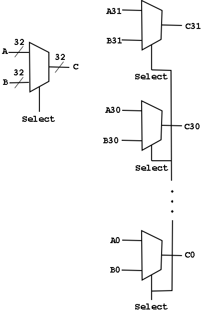
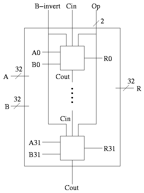
Arrays of Logic Elements
- Do the same thing to many signals
- Draw thicker lines and use the ``by n'' notation.
- Diagram below shows a 32-bit 2-way mux and an implementation with 32
1-bit, 2-way muxes.
- A Bus is a collection of data lines treated
as a single logical (n-bit) value.
- Use an array of logic elements to process a bus.
For example, the above mux switches between 2 32-bit buses.
*** Big Change Coming ***
Sequential Circuits, Memory, and State
Why do we want to have state?
- Memory (i.e. ram not just rom or prom)
- Counters
- Reducing gate count
- Multiplier would be quadradic in comb logic.
- With sequential logic (state) can do in linear.
- What follows is unofficial (i.e. too fast to
understand)
- Shift register holds partial sum
- Real slick is to share this shift reg with
multiplier
- We will do this circuit later in the course
Assume you have a real OR gate. Assume the two inputs are both
zero for an hour. At time t one input becomes 1. The output will
OSCILLATE for a while before settling on exactly 1. We want to be
sure we don't look at the answer before its ready.
B.4: Clocks

Frequency and period
- Hertz (Hz), Megahertz, Gigahertz vs. Seconds, Microseconds,
Nanoseconds
- Old (descriptive) name for Hz is cycles per second (CPS)
- Rate vs. Time
Edges
- Rising Edge; falling edge
- We use edge-triggered logic
- State changes occur only on a clock edge
- Will explain later what this really means
- One edge is called the Active edge
- The edge (rising or falling) on which changes occur
- Choice is technology dependent
- Sometimes trigger on both edges (e.g., RAMBUS or DDR memory)
Synchronous system
Now we are going to add state elements to the combinational
circuits we have been using previously.
Remember that a combinational/combinatorial circuits has its outpus
determined by its input, i.e. combinatorial circuits do not contain
state.
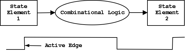
State elements include state (naturally).
- i.e., memory
- state-elements have clock as an input
- can change state only at active edge
- produce output Always; based on current state
- all signals that are written to state elements must be valid at
the time of the active edge.
- For example, if cycle time is 10ns make sure combinational circuit
used to compute new state values completes in 10ns
- So state elements change on active edge, comb circuit
stabilizes between active edges.
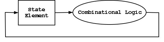
- Think of registers or memory as state elements.
- Can have loops like at the right.
- A loop like this is a cycle of the computer.
B.5: Memory Elements
We want edge-triggered clocked memory and will only use
edge-triggered clocked memory in our designs. However we get
there by stages. We first show how to build unclocked
memory; then using unclocked memory we build
level-sensitive clocked memory; finally from
level-sensitive clocked memory we build edge-triggered
clocked memory.
Unclocked Memory
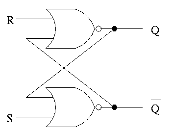
S-R latch (set-reset)
- ``Cross-coupled'' nor gates
- Don't assert both S and R at once
- When S is asserted (i.e., S=1 and R=0)
- the latch is Set (that's why it is called S)
- Q becomes true (Q is the output of the latch)
- Q' becomes false (Q' is the complemented output)
- When R is asserted
- the latch is Reset
- Q becomes false
- Q' becomes true
- When neither one is asserted
- The latch remains the same, i.e. Q and Q' stay as they
were
- This is the memory aspect
Clocked Memory: Flip-flops and latches
The S-R latch defined above is not clocked memory. Unfortunately the
terminology is not perfect.
For both flip-flops and
latches the output equals the value stored in the
structure. Both have an input and an output (and the complemented
output) and a clock input as well. The clock determines when the
internal value is set to the current input. For a latch, the change
occurs whenever the clock is asserted (level sensitive). For a
flip-flop, the change occurs at the active edge.
D latch
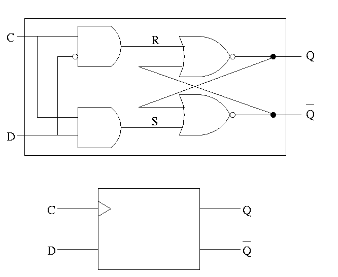
The D is for data
- The left part uses the clock.
- When the clock is low, both R and S are forced low.
- When the clock is high, S=D and R=D' so the value store is D.
- Output changes when input changes and the clock is asserted.
- Level sensitive rather than edge triggered.
- Sometimes called a transparent latch.
- We won't use these in designs.
- The right hand part of the circuit is the S-R (unclocked) latch we
just constructed.
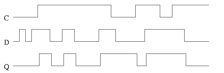
In the traces below notice how the output follows the input when the
clock is high and remains constant when the clock is low. We assume
the stored value is initially low.
D or Master-Slave Flip-flop
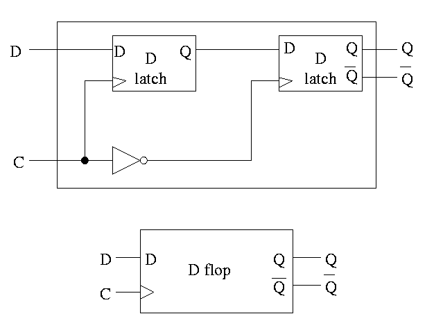
This was our goal. We now have an edge-triggered, clocked memory.
- Built from D latches, which are transparent
- The result is Not transparent
- Changes on the active edge
- This one has the falling edge as active edge
- Sometimes called a master-slave flip-flop
- Note substructures with letters reused
having different meaning (block structure a la algol)
- Master latch (the left one) is set during the time clock is
asserted.
Remember that the latch is transparent, i.e. follows
its input when its clock is asserted. But the second
latch is ignoring its input at this time. When the
clock falls, the 2nd latch pays attention and the
first latch keeps producing whatever D was at
fall-time.
- Actually D must remain constant for some time around
the active edge.
- The set-up time before the edge
- The hold time after the edge
- See diagram below
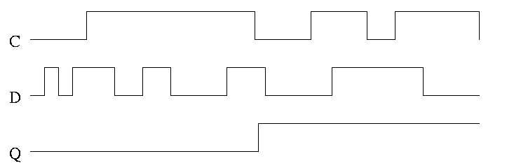
Note how much less wiggly the output is with the master-slave flop
than before with the transparent latch. As before we are assuming the
output is initially low.
Homework:
Try moving the inverter to the other latch
What has changed?
======== START LECTURE #5
========
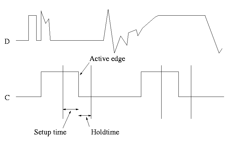
- This picture shows the setup and hold times discussed above.
- It is crucial when building circuits with flip flops that D is
stable during the interval between the setup and hold times.
- Note that D is wild outside the critical interval, but that is OK.
Homework:
B.18
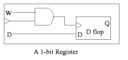
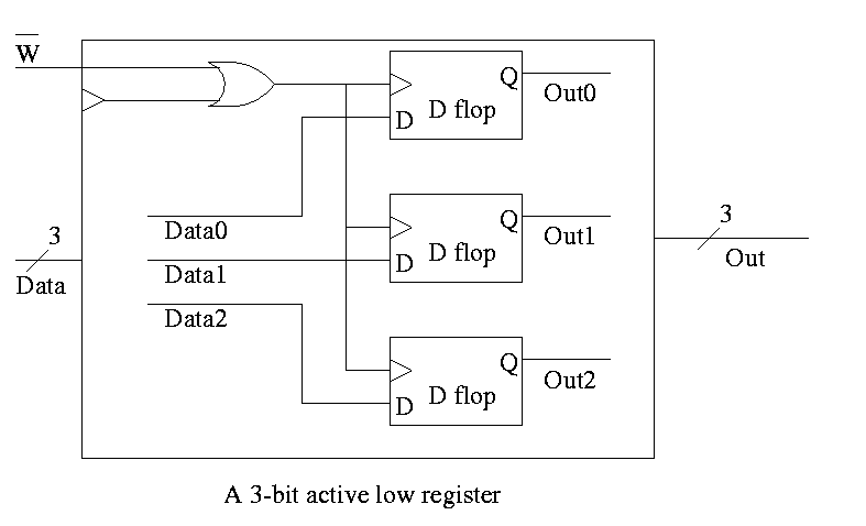
Registers
- Basically just an array of D flip-flops
- But what if you don't want to change the register during a
particular cycle?
- Introduce another input, the write line
- The write line is used to ``gate the clock''
- The book forgot the write line.
- Clearly if the write line is high forever, the clock input to
the register is passed right along to the D flop and hence the
input to the register is stored in the D flop when the active edge
occurs (for us the falling edge).
- Also clear is that if the write line is low forever, the clock
to the D flop is always low so has no edges and no writing occurs.
- But what about changing the write line?
- Assert or deassert the write line while the clock is low and
keep it at this value until the clock is low again.
- Not so good! Must have the write line correct quite a while
before the active edge. That is you must know whether you are
writing quite a while in advance.
- Better to do things so the write line must be correct when the
clock is high (i.e., just before the active edge
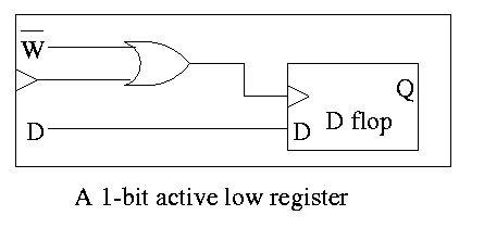
- An alternative is to use an active low write line,
i.e. have a W' input.
- Must have write line and data line valid during setup and hold
times
- To do a multibit register, just use multiple D flops.
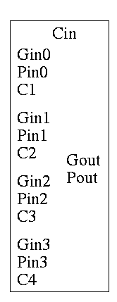
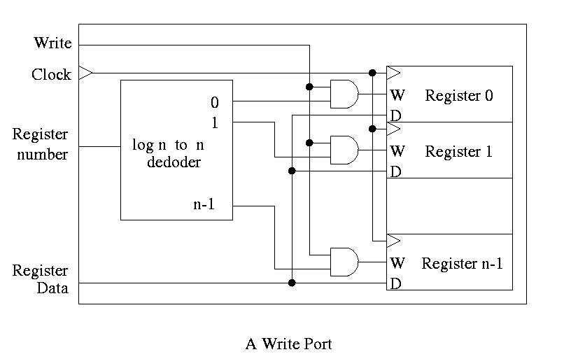
Register File
Set of registers each numbered
- Supply reg#, write line, and data (if a write)
- Can read and write same reg same cycle. You read the old value and
then the written value replaces this old value for subsequent cycles.
- Often have several read and write ports so that several
registers can be read and written during one cycle.
- We will do 2 read ports and one write port since that is
needed for ALU ops. This is Not adequate for superscalar (or
EPIC) or any other system where more than one operation is to be
calculated each cycle.
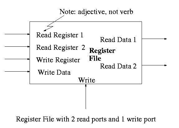
To read just need mux from register file to select correct
register.
- Have one of these for each read port
- Each is an n to 1 mux, b bits wide; where
- n is the number of registers (32 for MIPS)
- b is the width of each register (32 for MIPS)
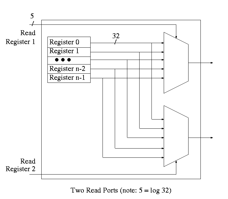
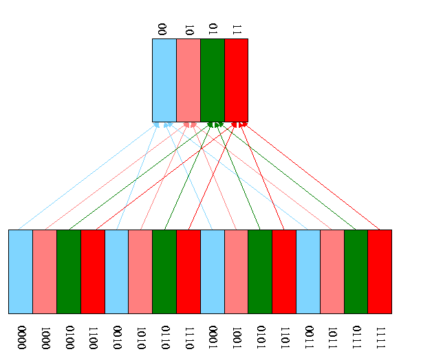
For writes use a decoder on register number to determine which
register to write. Note that 3 errors in the book's figure were fixed
- decoder is log n to n
- decoder outputs numbered 0 to n-1 (NOT n)
- clock is needed
The idea is to gate the write line with the output of the decoder. In
particular, we should perform a write to register r this cycle providing
- Recall that the inputs to a register are W, the write line, D the
data to write (if the write line is asserted) and the clock.
- The clock to each register is simply the clock input to the
register file.
- The data to each register is simply the write data to the register file.
- The write line to each register is unique
- The register number is fed to a decoder.
- The rth output of the decoder is asserted if r is the
specified register.
- Hence we wish to write register r if
- The write line to the register file is asserted
- The rth output of the decoder is asserted
- Bingo! We just need an and gate.
Homework: 20
======== START LECTURE #6
========
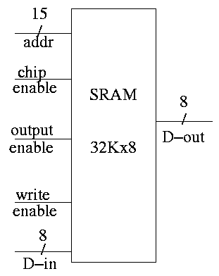
SRAMS and DRAMS
- External interface is on right
- 32Kx8 means it hold 32K words each 8 bits.
- Addr, D-in, and D-out are same as registers. Addr is 15
bits since 2 ^ 15 = 32K. D-out is 8 bits since we have a by 8
SRAM.
- Write enable is similar to the write line (unofficial: it
is a pulse; there is no clock),
- Output enable is for the three state (tri-state) drivers
discussed just below (unofficial).
- Ignore chip enable (perfer not to have all chips enabled
for electrical reasons).
- (Sadly) we will not look inside officially. Following is
unofficial
- Conceptually, an SRAM is like a register file but we can't
use the register file implementation for a large SRAM because
there would be too many wires and the muxes would be too big.
- Two stage decode.
- For a 32Kx8 SRAM would need a 15-32K decoder.
- Instead package the SRAM as eight 512x64 SRAMS.
- Pass 9 bits of the address through a 9-512 decoder and
use these 512 wires to select the appropriate 64-bit word
from each of the sub SRAMS. Use the remaining 6 bits to
select the appropriate bit from each 64-bit word.
- Tri-state buffers (drivers) used instead of a mux.
- I was fibbing when I said that signals always have a 1 or 0.
- However, we will not use tristate logic; we will use muxes.
- DRAM uses a version of the above two stage decode.
- View the memory as an array.
- First select (and save in a ``faster'' memory) an
entire row.
- Then select and output only one (or a few) column(s).
- So can speed up access to elts in same row.
- SRAM and ``logic'' are made from similar technologies but
DRAM technology is quite different.
- So easy to merge SRAM and CPU on one chip (SRAM
cache).
- Merging DRAM and CPU is more difficult but is now
being done.
- Error Correction (Omitted)
Note:
There are other kinds of flip-flops T, J-K. Also one could learn
about excitation tables for each. We will not cover this
material (H&P doesn't either). If interested, see Mano
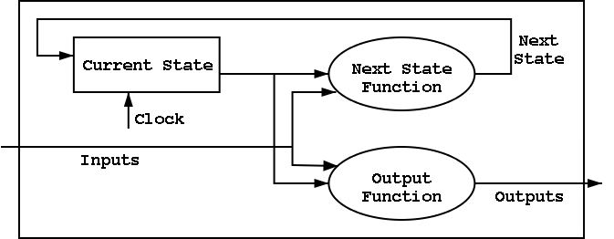
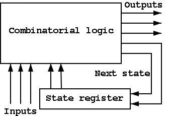
B.6: Finite State Machines
I do a different example from the book (counters instead of traffic
lights). The ideas are the same and the two generic pictures (below)
apply to both examples.
Counters
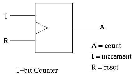
A counter counts (naturally).
- The counting is done in binary.
- Increments (i.e., counts) on clock ticks (active edge).
- Actually only on those clocks ticks when the ``increment'' line is
asserted.
- If reset asserted at a clock tick, the counter is reset to zero.
- What if both reset and increment assert?
Ans: Shouldn't do that. Will accept any answer (i.e., don't care).
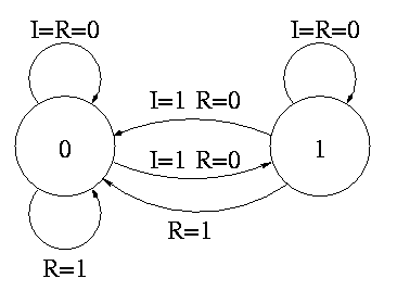
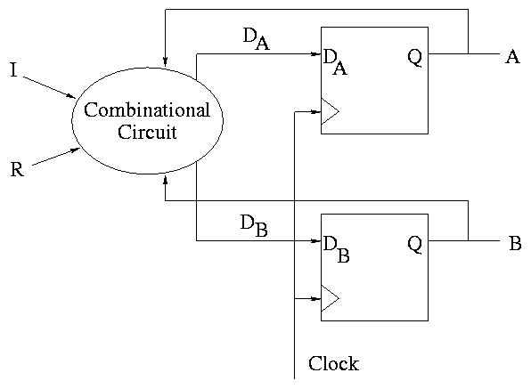
The state transition diagram
- The figure shows the state transition diagram for A, the output of
a 1-bit counter.
- In this implementation, if R=I=1 we choose to set A to zero. That
is, if Reset and Increment are both asserted, we do the Reset.
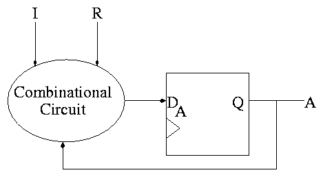
The circuit diagram.
- Uses one flop and a combinatorial circuit.
- The (combinatorial) circuit is determined by the transition diagram.
- The circuit must calculate the next value of A from the current
value and I and R.
- The flop producing A is often itself called A and the D input to this
flop is called DA (really D sub A).
How do we determine the combinatorial circuit?
- This circuit has three inputs, I, R, and the current A.
- It has one output, DA, which is the desired next A.
- So we draw a truth table, as before.
- For convenience I added the label Next A to the DA column
Current      || Next A
   A    I R  || DA <-- i.e. to what must I set DA
-------------++--      in order to get the desired
   0    0 0  || 0      Next A for the next cycle.
   1    0 0  || 1
   0    1 0  || 1
   1    1 0  || 0
   x    x 1  || 0
But this table is simply the truth table for the combinatorial
circuit.
A I R  || DA
-------++--
0 0 0  || 0
1 0 0  || 1
0 1 0  || 1
1 1 0  || 0
x x 1  || 0

DA = R' (A XOR I)
How about a two bit counter.
- State diagram has 4 states 00, 01, 10, 11 and transitions from one
to another
- The circuit diagram has 2 D flops
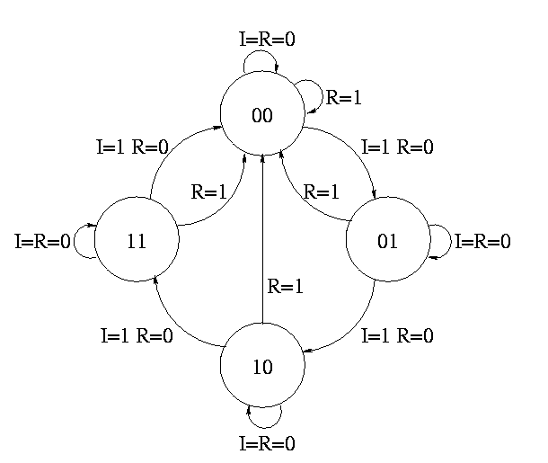
To determine the combinatorial circuit we could precede as before
Current      ||
  A B   I R  || DA DB
-------------++------
This would work but we can instead think about how a counter works and
see that.
DA = R'(A XOR I)
DB = R'(B XOR AI)
Homework: B.23
B.7 Timing Methodologies
Skipped
======== START LECTURE #7
========
Simulating Combinatorial Circuits at the Gate Level
The idea is, given a circuit diagram, write a program that behaves the
way the circuit does. This means more than getting the same answer.
The program is to work the way the circuit does.
For each logic box, you write a procedure with the following properties.
- A parameters is defined for each input and output wire.
- A (local) variable is defined for each internal wire.
Really means a variable define for each signal. If a signal is
sent from one gate to say 3 others, you might not call all those
connections one wire, but it is one signal and is represented by
one variable
- The only operations used are AND OR XOR NOT
- In the C language & | ^ ! (do NOT use ~)
- Other languages similar.
- Best is a language with variables and constants of type Boolean.
- An assignment statement (with an operator) corresponds to a
gate.
For example A = B & C; would mean that there is an AND gate with
input wires B and C and output wire A.
- NO conditional assignment.
- NO if then else statements.
Implement a mux using ANDs, ORs, and NOTs.
- Single assignment to each variable.
Multiple assignments would correspond to a cycle or to two outputs
connected to the same wire.
- A bus (i.e., a set of signals) is represented by an array.
- Testing
- Exhaustive possible for 1-bit cases.
- Cleverness for n-bit cases (n=32, say).
Simulating a Full Adder
Remember that a full adder has three inputs and two outputs. Hand
out hard copies of
FullAdder.c.
Simulating a 4-bit Adder
This implementation uses the full adder code above. Hand out hard
copies of FourBitAdder.c.
Lab 1: Simulating A 1-bit ALU
Hand out Lab 1, which is available in
text (without the diagram),
pdf, and
postscript.
Chapter 1: Computer Abstractions and Technologies
Homework:
READ chapter 1. Do 1.1 -- 1.26 (really one matching question)
Do 1.27 to 1.44 (another matching question),
1.45 (and do 10,000 RPM),
1.46, 1.50
Chapter 3: Instructions: Language of the Machine
Homework:
Read sections 3.1 3.2 3.3
3.4 Representing instructions in the Computer (MIPS)
Register file
- We just learned how to build this
- 32 Registers each 32 bits
- Register 0 is always 0 when read and stores to register 0 are ignored
Homework:
3.2.
The fields of a MIPS instruction are quite consistent
    op    rs    rt    rd    shamt  funct   <-- name of field
    6     5     5     5      5      6      <-- number of bits
- op is the opcode
- rs,rt are source operands
- rd is destination
- shamt is the shift amount
- funct is used for op=0 to distinguish alu ops
- alu is arithmetic and logic unit
- add/sub/and/or/not etc.
- We will see there are other formats (but similar to this one).
R-type instruction (R for register)
Example: add $1,$2,$3
- R-type use the format above
- The example given has for its 6 fields
0--2--3--1--0--32
- op=0, alu op
- funct=32 specifies add
- reg1 <-- reg2 + reg3
- The regs can all be the same (doubles the value in the reg).
- Do sub by just changing the funct
- If the regs are the same for subtract, the instruction clears the register.
I-type (why I?)
    op    rs    rt   address
    6     5     5     16
- rs is a source reg.
- rt is the destination reg.
Examples: lw/sw $1,1000($2)
- $1 <-- Mem[$2+1000]
$1 --> Mem[$2+1000]
- Transfers to/from memory, normally in words (32-bits)
- But the machine is byte addressable!
- Then how come have load/store word instead of byte?
Ans: It has load/store byte as well, but we don't cover it.
- What if the address is not a multiple of 4D?
Ans: An error (MIPS requires aligned accesses).
- machine format is: 35/43 $2 $1 1000
RISC-like properties of the MIPS architecture.
- All instructions are the same length (32 bits).
- Field sizes of R-type and I-type correspond.
- The type (R-type, I-type, etc.) is determined by the opcode.
- rs is the reference to memory for both load and store.
- These properties will prove helpful when we construct a MIPS processor.
Branching instruction
slt (set less-then)
Example: slt $3,$8,$2
- R-type
- reg3 <-- (if reg8 < reg2 then 1 else 0)
- Like other R-types: read 2nd and 3rd reg, write 1st
beq and bne (branch (not) equal)
Examples: beq/bne $1,$2,123
- I-type
- if reg1=reg2 then go to the 124rd instruction after this one.
- if reg1!=reg2 then go to the 124rd instruction after this one.
- Why 124 not 123?
Ans: We will see that the CPU adds 4 to the program counter (for
the no branch case) and then adds (4 times) the third operand.
- Normally one writes a label for the third operand and the
assembler calculates the offset needed.
======== START LECTURE #8
========
blt (branch if less than)
Examples: blt $5,$8,123
- I-type
- if reg5 < reg8 then go to the 124rd instruction after this one.
- *** WRONG ***
- There is no blt instruction.
- Instead use
    stl $1,$5,$8
    bne $1,$0,123
ble (branch if less than or equal)
- There is no ``ble $5,$8,L'' instruction.
- There is also no ``sle $1,$5,$8'' set $1 if $5 less or equal $8.
- Note that $5<=$8 <==> NOT ($8<$5).
- Hence we test for $8<$5 and branch if false.
    stl $1,$8,$5
    beq $1,$0,L
bgt (branch if greater than>
- There is no ``bgt $5,$8,L'' instruction.
- There is also no ``sgt $1,$5,$8'' set $1 if $5 greater than $8.
- Note that $5>$8 <==> $8<$5.
- Hence we test for $8<$5 and branch if true.
    stl $1,$8,$5
    bne $1,$0,L
bge (branch if greater than or equal>
- There is no ``bge $5,$8,L'' instruction.
- There is also no ``sge $1,$5,$8'' set $1 if $5 greater or equal $8l
- Note that $5>=$8 <==> NOT ($5<$8)l
- Hence we test for $5<$8 and branch if false.
    stl $1,$5,$8
    beq $1,$0,L
Note:
Please do not make the mistake of thinking that
    stl $1,$5,$8
    beq $1,$0,L
is the same as
    stl $1,$8,$5
    bne $1,$0,L
The negation of X < Y is not Y < X
End of Note
Homework:
3.12
J-type instructions (J for jump)
        op   address
        6     26
j (jump)
Example: j 10000
- Jump to instruction (not byte) 10000.
- Branches are PC relative, jumps are absolute.
- J type
- Range is 2^26 words = 2^28 bytes = 1/4 GB
jr (jump register)
Example: jr $10
- Jump to the location in register 10.
- R type, but uses only one register.
- Will it use one of the source registers or the destination register?
Ans: This will be obvious when we construct the processor.
jal (jump and link)
Example: jal 10000
- Jump to instruction 10000 and store the return address (the
address of the instruction after the jal).
- Used for subroutine calls.
- J type.
- Return address is stored in register 31. By using a fixed
register, jal avoids the need for a second register field and hence
can have 26 bits for the instruction address (i.e., can be a J type).
I type instructions (revisited)
- The I is for immediate.
- These instructions have an immediate third operand,
i.e., the third operand is contained in the instruction itself.
- This means the operand itself, and not just its address or register
number, is contained in the instruction.
- Two registers and one immediate operand.
- Compare I and R types: Since there is no shamt and no funct, the
immediate field can be larger than the field for a register.
- Recall that lw and sw were I type. They had an immediate operand,
the offset added to the register to specify the memory address.
addi (add immediate)
Example: addi $1,$2,100
- $1 = $2 + 100
- Why is there no subi?
Ans: Make the immediate operand negative.
slti (set less-than immediate)
Example slti $1,$2,50
- Set $1 to 1 if $2 less than 50; set $1 to 0 otherwise.
lui (load upper immediate)
Example: lui $4,123
- Loads 123 into the upper 16 bits of register 4 and clears the
lower 16 bits of the register.
- What is the use of this instruction?
- How can we get a 32-bit constant into a register since we can't
have a 32 bit immediate?
- Load the word
- Have the constant placed in the program text (via some
assembler directive).
- Issue lw to load the register.
- But memory accesses are slow and this uses a cache entry.
- Load shift add
- Load immediate the high order 16 bits (into the low order
of the register).
- Shift the register left 16 bits (filling low order with
zero)
- Add immediate the low order 16 bits
- Three instructions, three words of memory
- load-upper add
- Use lui to load immediate the desired 16-bit value into
the high order 16 bits of the register and clear the low
order bits.
- Add immediate the desired low order 16 bits.
- lui $4,123 -- puts 123 into top half of register 4.
addi $4,$4,456 -- puts 456 into bottom half of register 4.
Homework:
3.1, 3.3, 3.4, and 3.5.
Chapter 4
Homework:
Read 4.1-4.4
4.2: Signed and Unsigned Numbers
MIPS uses 2s complement (just like 8086)
To form the 2s complement (of 0000 1111 0000 1010 0000 0000 1111 1100)
- Take the 1s complement.
- That is, complement each bit (1111 0000 1111 0101 1111 1111 0000 0011)
- Then add 1 (1111 0000 1111 0101 1111 1111 0000 0100)
Need comparisons for signed and unsigned.
- For signed a leading 1 is smaller (negative) than a leading 0
- For unsigned a leading 1 is larger than a leading 0
sltu and sltiu
Just like slt and slti but the comparison is unsigned.
Homework:
4.1-4.9
4.3: Addition and subtraction
To add two (signed) numbers just add them. That is don't treat
the sign bit special.
To subtract A-B, just take the 2s complement of B and add.
Overflows
An overflow occurs when the result of an operatoin cannot be
represented with the available hardware. For MIPS this means when the
result does not fit in a 32-bit word.
- We have 31 bits plus a sign bit.
- The result would definitely fit in 33 bits (32 plus sign)
- The hardware simply discards the carry out of the top (sign) bit
- This is not wrong--consider -1 + -1
  11111111111111111111111111111111   (32 ones is -1)
+ 11111111111111111111111111111111
----------------------------------
 111111111111111111111111111111110   Now discard the carry out

  11111111111111111111111111111110   this is -2
- The bottom 31 bits are always correct.
Overflow occurs when the 32 (sign) bit is set to a value and not
the sign.
- Here are the conditions for overflow
Operation  Operand A  Operand B  Result
   A+B       >= 0        >= 0      < 0
   A+B        < 0         < 0     >= 0
   A-B       >= 0         < 0      < 0
   A-B        < 0        >= 0     >= 0
- These conditions are the same as
Carry-In to sign position != Carry-Out
Homework:
Prove this last statement (4.29)
(for fun only, do not hand in).
addu, subu, addiu
These add and subtract the same as add and sub,
but do not signal overflow
4.4: Logical Operations
Shifts: sll, srl
- R type, with shamt used and rs not used.
- sll $1,$2,5
reg2 gets reg1 shifted left 5 bits.
- Why do we need both sll and srl,
i.e, why not just have one of them and use a negative
shift amt for the other?
Ans: The shift amt is only 5 bits and need shifts from 0 to 31
bits. Hence not enough bits for negative shifts.
- These are shifts not rotates.
- Op is 0 (these are ALU ops, will understand why in a few weeks).
Bitwise AND and OR: and, or, andi, ori
No surprises.
- and $r1,$r2,$r3
or $r1,$r2,$r3
- standard R-type instruction
- andi $r1,$r2,100
ori $r1,$r2,100
- standard I-type
4.5: Constructing an ALU--the fun begins
First goal is 32-bit AND, OR, and addition
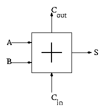
Recall we know how to build a full adder. We will draw it as shown on
the right.
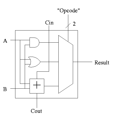
With this adder, the ALU is easy.
- Just choose the correct operation (ADD, AND, OR)
- Note the principle that if you want a logic box that sometimes
computes X and sometimes computes Y, what you do is
- Always compute X.
- Always compute Y.
- Put both X and Y into a mux.
- Use the ``sometimes'' condition as the select line to the mux.
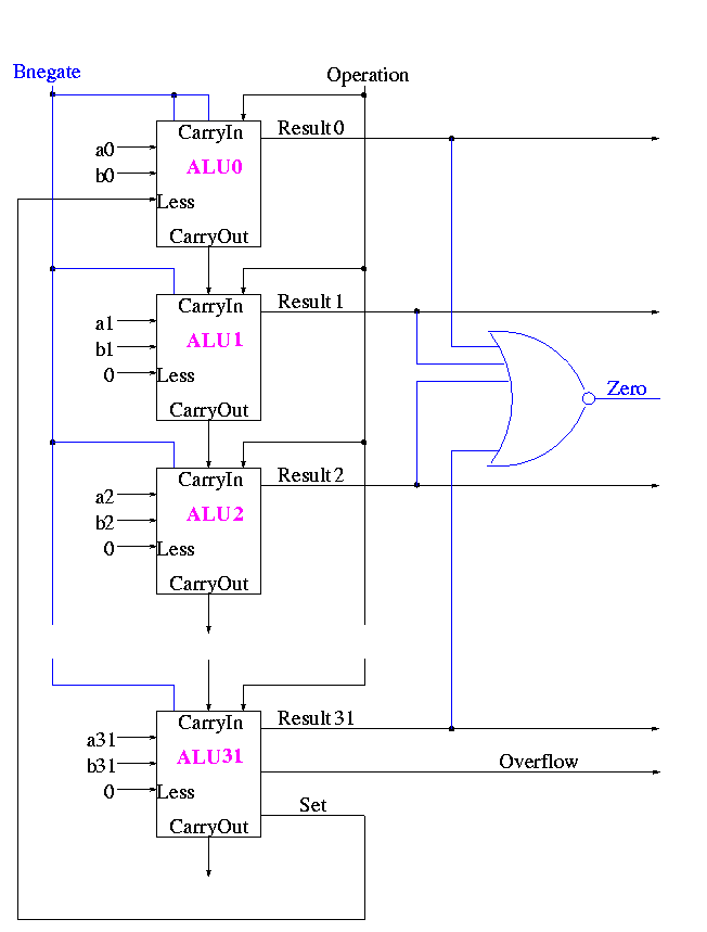
With this 1-bit ALU, constructing a 32-bit version is simple.
- Use an array of logic elements for the logic. The logic element
is the 1-bit ALU
- Use buses for A, B, and Result.
- ``Broadcast'' Opcode to all of the internal 1-bit ALUs. This
means wire the external Opcode to the Opcode input of each of the
internal 1-bit ALUs
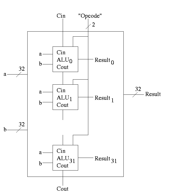
First goal accomplished.
======== START LECTURE #9
========
Now we augment the ALU so that we can perform subtraction (as well
as addition, AND, and OR).
- Big deal about 2's compliment is that
A - B = A + (2's comp B) = A + (B' + 1).
- Get B' from an inverter (naturally).
- Get +1 from the Carry-In.
1-bit ALU with ADD, SUB, AND, OR is

Implementing addition and subtraction
- To implement addition we use opcode 10 as before and de-assert
both b-invert and Cin.
- To implement subtraction we still use opcode 10 but we assert
both b-invert and Cin.
32-bit version is simply a bunch of these.
- For subtraction assert both B-invert and Cin.
- For addition de-assert both B-invert and Cin.
- For AND and OR de-assert B-invert. Cin is a don't care.
- We get for free A+B'
If we let A=0, this gives B', i.e. the NOT operation
However, we will not use it. Indeed we will soon give it away.
(More or less) all ALUs do AND, OR, ADD, SUB.
Now we want to customize our ALU for the MIPS architecture.
Extra requirements for MIPS ALU:
-
slt set-less-than
-
Result reg is 1 if a < b
Result reg is 0 if a >= b
-
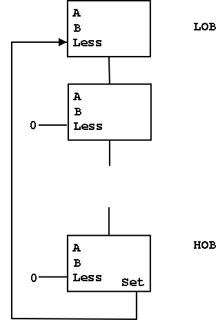
So need to set the LOB (low order bit, aka least significant bit)
of the result equal to the sign bit of a subtraction, and set the
rest of the result bits to zero.
-
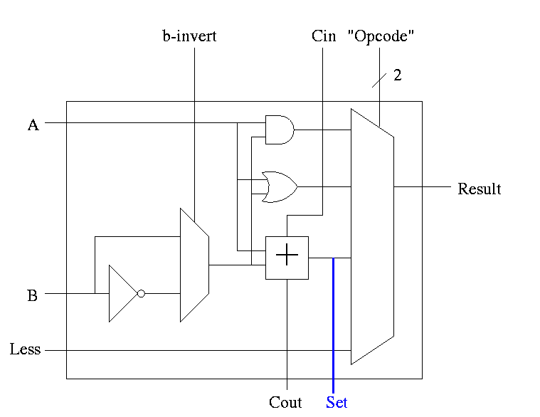
Idea #1. Give the mux another input, called LESS.
This input is brought in from outside the bit cell.
That is, if the opcode is slt we make the select line to the
mux equal to 11 (three) so that the the output is the this new
input. For all the bits except the LOB, the LESS input is
zero. For the LOB we must figure out how to set LESS.
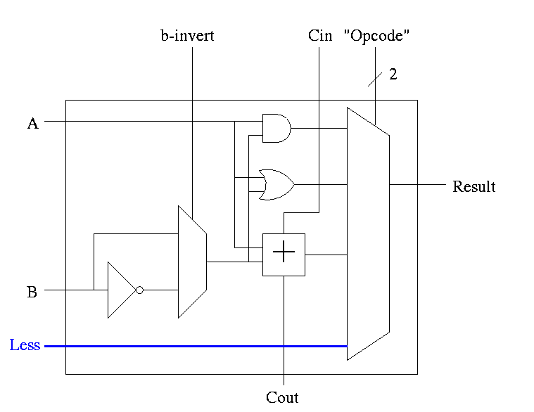
-
Idea #2. Bring out the result of the adder (BEFORE the mux)
Only needed for the HOB (high order bit, i.e. sign) Take this
new output from the HOB, call it SET and connect it to the
LESS input in idea #1 for the LOB. The LESS input for other
bits are set to zero.
-
Why isn't this method used?
-
Ans: It is wrong!
-
Example using 3 bit numbers (i.e. -4 .. 3).
- Try slt on -3 and +2.
- True subtraction (-3 - +2) gives -5.
- The negative sign in -5 indicates (correctly) that -3 < +2.
- But three bit subtraction -3 - +2 gives +3 !
- Hence we will incorrectly conclude that -3 is NOT less than +2.
- (Really, the subtraction signals an overflow.
unless doing unsigned)
-
Solution: Need the correct rule for less than (not just sign of
subtraction).
Homework: figure out correct rule, i.e. prob 4.23.
Hint: when an overflow occurs the sign bit is definitely wrong (so the
complement of the sign bit is right).
-
Overflows
- The HOB ALU is already unique (outputs SET).
- Need to enhance it some more to produce the overflow output.
- Recall that we gave the rule for overflow. You need to examine:
- Whether the operation is add or sub (binvert).
- The sign of A.
- The sign of B.
- The sign of the result.
- Since this is the HOB we have all the sign bits.
- The book also uses Cout, but this appears to be an error.
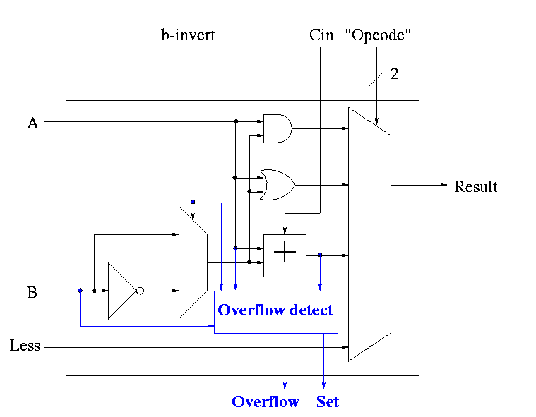
- Simpler overflow detection.
- An overflow occurs if and only if the carry in to the HOB
differs from the carry out of the HOB.
-
Zero Detect
- To see if all bits are zero just need NOR of all the bits
- Conceptually trivially but does require some wiring
-
Observation: The CarryIn to the LOB and Binvert
to all the 1-bit ALUs are always the same.
So the 32-bit ALU has just one input called Bnegate, which is sent
to the appropriate inputs in the 1-bit ALUs.
The Final Result is
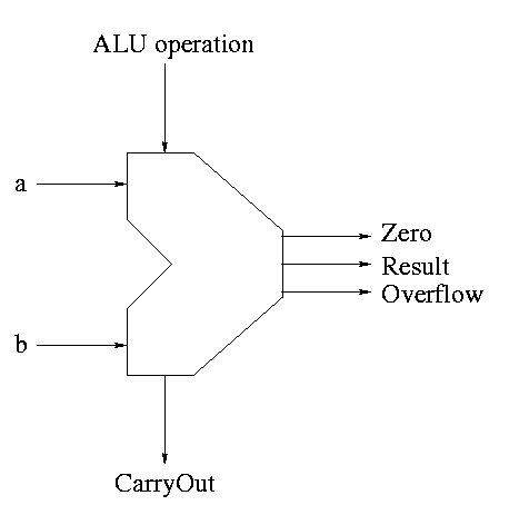
The symbol used for an ALU is on the right
What are the control lines?
-
Bnegate (1 bit)
-
OP (2 bits)
What functions can we perform?
-
and
-
or
-
add
-
sub
-
set on less than
What (3-bit) values for the control lines do we need for each
function? The control lines are Bnegate (1-bit) and Operation (2-bits)
| and | 0 | 00 |
| or | 0 | 01 |
| add | 0 | 10 |
| sub | 1 | 10 |
| slt | 1 | 11 |
======== START LECTURE #10
========
Fast Adders
-
We have done what is called a ripple carry adder.
- The carry ``ripples'' from one bit to the next (LOB to HOB).
- So the time required is proportional to the wordlength
- Each carry can be computed with two levels of logic (any function
can be so computed) hence the number of gate delays for an n bit
adder is 2n.
- For a 4-bit adder 8 gate delays are required.
- For an 16-bit adder 32 gate delays are required.
- For an 32-bit adder 64 gate delays are required.
- For an 64-bit adder 128 gate delays are required.
-
What about doing the entire 32 (or 64) bit adder with 2 levels of
logic?
-
Such a circuit clearly exists. Why?
Ans: A two levels of logic circuit exists for any
function.
-
But it would be very expensive: many gates and wires.
-
The big problem: When expressed with two levels of
login, the AND and OR gates have high
fan-in, i.e., they have a large number of inputs. It is
not true that a 64-input AND takes the same time as a
2-input AND.
-
Unless you are doing full custom VLSI, you get a toolbox of
primative functions (say 4 input NAND) and must build from that
-
There are faster adders, e.g. carry lookahead and carry save. We
will study carry lookahead adders.
Carry Lookahead Adder (CLA)
This adder is much faster than the ripple adder we did before,
especially for wide (i.e., many bit) addition.
- For each bit position we have two input bits, a and b (really
should say ai and bi as I will do below).
- We can, in one gate delay, calculate two other bits
called generate g and propagate p, defined as follows:
- The idea for propagate is that p is true if the
current bit will propagate a carry from its input to its output.
- It is easy to see that p = (a OR b), i.e.
if and only if (a OR b)
then if there is a carry in
then there is a carry out
- The idea for generate is that g is true if the
current bit will generate a carry out (independent of the carry in).
- It is easy to see that g = (a AND b), i.e.
if and only if (a AND b)
then the must be a carry-out independent of the carry-in
To summarize, using a subscript i to represent the bit number,
    to generate  a carry:   gi = ai bi
    to propagate a carry:   pi = ai+bi
H&P give a plumbing analogue
for generate and propagate.
Given the generates and propagates, we can calculate all the carries
for a 4-bit addition (recall that c0=Cin is an input) as follows (this
is the formula version of the plumbing):
c1 = g0 + p0 c0

c2 = g1 + p1 c1 = g1 + p1 g0 + p1 p0 c0

c3 = g2 + p2 c2 = g2 + p2 g1 + p2 p1 g0 + p2 p1 p0 c0

c4 = g3 + p3 c3 = g3 + p3 g2 + p3 p2 g1 + p3 p2 p1 g0 + p3 p2 p1 p0 c0
Thus we can calculate c1 ... c4 in just two additional gate delays
(where we assume one gate can accept upto 5 inputs). Since we get gi
and pi after one gate delay, the total delay for calculating all the
carries is 3 (this includes c4=Carry-Out)
Each bit of the sum si can be calculated in 2 gate delays given ai,
bi, and ci. Thus, for 4-bit addition, 5 gate delays after we are
given a, b and Carry-In, we have calculated s and Carry-Out.
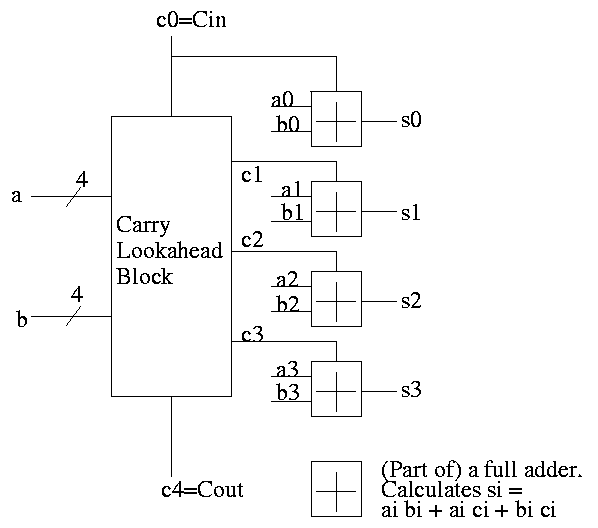
So, for 4-bit addition, the faster adder takes time 5 and the slower
adder time 8.
Now we want to put four of these together to get a fast 16-bit
adder.
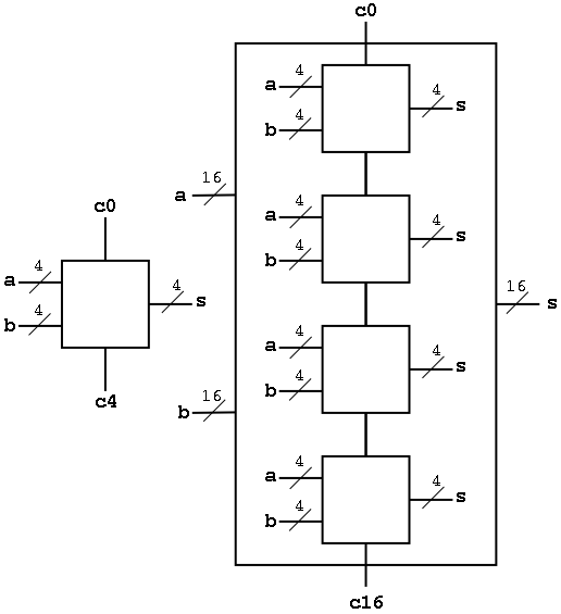
As black boxes, both ripple-carry adders and carry-lookahead adders
(CLAs) look the same.
We could simply put four CLAs together and let the Carry-Out from
one be the Carry-In of the next. That is, we could put these CLAs
together in a ripple-carry manner to get a hybrid 16-bit adder.
- Since the Carry-Out is calculated in 3 gate delays, the Carry-In to
the high order 4-bit adder is calculated in 3*3=9 delays.
- Hence the overall Carry-Out takes time 9+3=12 and the high order
four bits of the sum take 9+5=14. The other bits take less time.
- So this mixed 16-bit adder takes 14 gate delays compared with
2*16=32 for a straight ripple-carry 16-bit adder.
We want to do better so we will put the 4-bit carry-lookahead
adders together in a carry-lookahead manner. Thus the diagram above
is not what we are going to do.
- We have 33 inputs a0,...,a15; b0,...b15; c0=Carry-In
- We want 17 outputs s0,...,s15; c16=c=Carry-Out
- Again we are assuming a gate can accept upto 5 inputs.
- It is important that the number of inputs per gate does not grow
with the number of bits in each number.
- If the technology available supplies only 4-input gates (instead
of the 5-input gates we are assuming),
we would use groups of three bits rather than four
We start by determining ``super generate'' and ``super propagate''
bits.
- The super generate indicates whether the 4-bit
adder constructed above generates a Carry-Out.
- The super propagate indicates whether the 4-bit
adder constructed above propagates a
Carry-In to a Carry-Out.
P0 = p3 p2 p1 p0          Does the low order 4-bit adder
                          propagate a carry?
P1 = p7 p6 p5 p4

P2 = p11 p10 p9 p8

P3 = p15 p14 p13 p12      Does the high order 4-bit adder
                          propagate a carry?


G0 = g3 + p3 g2 + p3 p2 g1 + p3 p2 p1 g0        Does low order 4-bit
                                                adder generate a carry
G1 = g7 + p7 g6 + p7 p6 g5 + p7 p6 p5 g4

G2 = g11 + p11 g10 + p11 p10 g9 + p11 p10 p9 g8

G3 = g15 + p15 g14 + p15 p14 g13 + p15 p14 p13 g12

From these super generates and super propagates, we can calculate the
super carries, i.e. the carries for the four 4-bit adders.
- The first super carry
C0, the Carry-In to the low-order 4-bit adder, is just c0 the input
Carry-In.
- The second super carry C1 is the Carry-Out of the low-order 4-bit
adder (which is also the Carry-In to the 2nd 4-bit adder.
- The last super carry C4 is the Carry-out of the high-order 4-bit
adder (which is also the overall Carry-out of the entire 16-bit adder).
C1 = G0 + P0 c0

C2 = G1 + P1 C1 = G1 + P1 G0 + P1 P0 c0

C3 = G2 + P2 C2 = G2 + P2 G1 + P2 P1 G0 + P2 P1 P0 c0

C4 = G3 + P3 C3 = G3 + P3 G2 + P3 P2 G1 + P3 P2 P1 G0 + P3 P2 P1 P0 c0
Now these C's (together with the original inputs a and b) are just
what the 4-bit CLAs need.
How long does this take, again assuming 5 input gates?
- We calculate the p's and g's (lower case) in 1 gate delay (as with
the 4-bit CLA).
- We calculate the P's one gate delay after we have the p's or
2 gate delays after we start.
- The G's are determined 2 gate delays after we have the g's and
p's. So the G's are done 3 gate delays after we start.
- The C's are determined 2 gate delays after the P's and G's. So
the C's are done 5 gate delays after we start.
- Now the C's are sent back to the 4-bit CLAs, which have already
calculated the p's and g's. The C's are calculated in 2 more
gate delays (7 total) and the s's 2 more after that (9 total).
In summary, a 16-bit CLA takes 9 cycles instead of 32 for a ripple carry
adder and 14 for the mixed adder.
Some pictures follow.
Take our original picture of the 4-bit CLA and collapse
the details so it looks like.
Next include the logic to calculate P and G.
Now put four of these with a CLA block (to calculate C's from P's,
G's and Cin) and we get a 16-bit CLA. Note that we do not use the Cout
from the 4-bit CLAs.
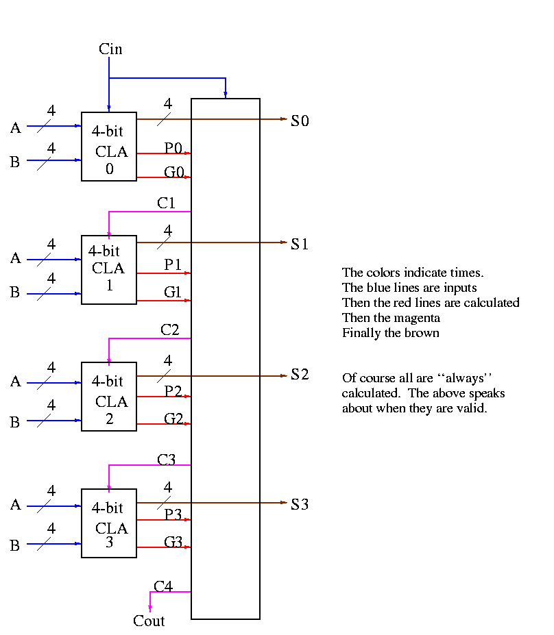
Note that the tall skinny box is general. It takes 4 Ps 4Gs and
Cin and calculates 4Cs. The Ps can be propagates, superpropagates,
superduperpropagates, etc. That is, you take 4 of these 16-bit CLAs
and the same tall skinny box and you get a 64-bit CLA.
Homework:
4.44, 4.45
As noted just above the tall skinny box is useful for all size
CLAs. To expand on that point and to review CLAs, let's redo CLAs with
the general box.
Since we are doing 4-bits at a time, the box takes 9=2*4+1 input bits
and produces 6=4+2 outputs
A 4-bit adder is now
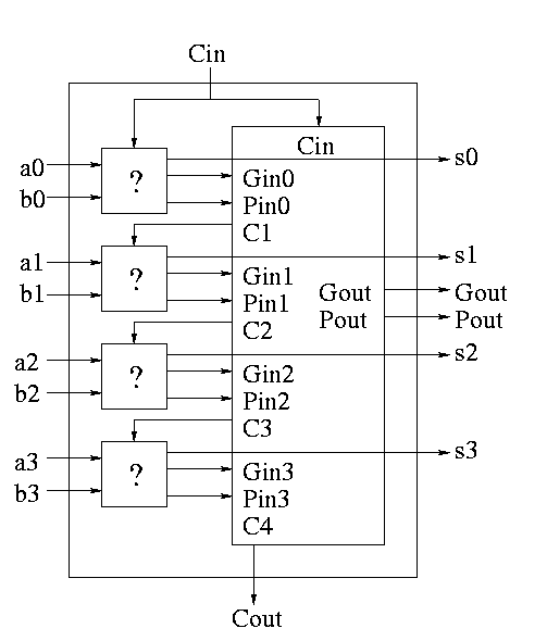
What does the ``?'' box do?
- Calculates Gi and Pi based on ai and bi
- Calculate s1 based on ai, bi, and Ci=Cin (normal full adder)
- Do not bother calculating Cout
Now take four of these 4-bit adders and use the identical
CLA box to get a 16-bit adder
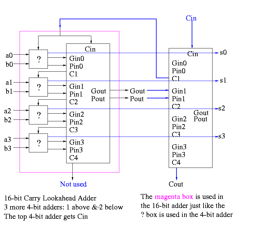
Four of these 16-bit adders with the identical
CLA box to gives a 64-bit adder.
======== START LECTURE #11
========
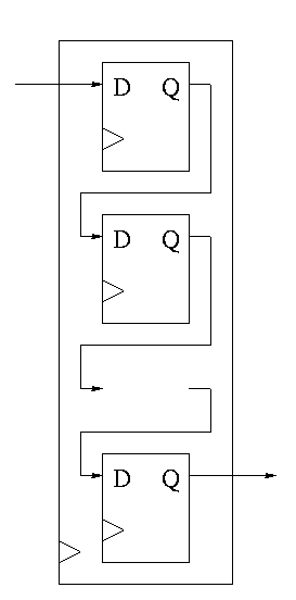
Shifter
This is a sequential circuit.
-
Just a string of D-flops; output of one is input of next
-
Input to first is the serial input.
-
Output of last is the serial output.
-
We want more.
-
Left and right shifting (with serial input/output)
-
Parallel load
-
Parallel Output
-
Don't shift every cycle
-
Parallel output is just wires.
-
Shifter has 4 modes (left-shift, right-shift, nop, load) so
-
4-1 mux inside
-
2 control lines must come in
-
We could modify our registers to be shifters (bigger mux), but ...
-
Our shifters are slow for big shifts; ``barrel shifters'' are
better and kept separate from the processor registers.
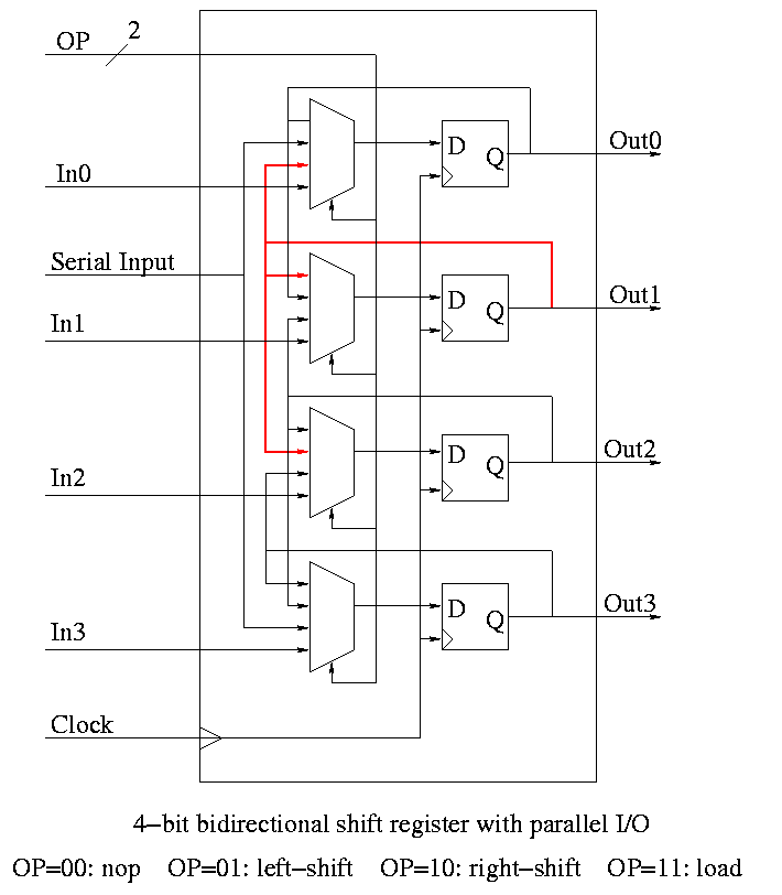
Homework:
A 4-bit shift register initially contains 1101. It is
shifted six times to the right with the serial input being
101101. What is the contents of the register after each
shift.
Homework:
Same register, same initial condition. For
the first 6 cycles the opcodes are left, left, right, nop,
left, right and the serial input is 101101. The next cycle
the register is loaded (in parallel) with 1011. The final
6 cycles are the same as the first 6. What is the contents
of the register after each cycle?
4.6: Multiplication
- Of course we can do this with two levels of logic since
multiplication is just a function of its inputs.
- But just as with addition, would have a very big circuit and large
fan in. Instead we use a sequential circuit that mimics the
algorithm we all learned in grade school.
-
Recall how to do multiplication.
-
Multiplicand times multiplier gives product
-
Multiply multiplicand by each digit of multiplier
-
Put the result in the correct column
-
Then add the partial products just produced
-
We will do it the same way ...
... but differently
-
We are doing binary arithmetic so each ``digit'' of the
multiplier is 1 or zero.
-
Hence ``multiplying'' the mulitplicand by a digit of the
multiplier means either
-
Getting the multiplicand
-
Getting zero
-
Use an ``if appropriate bit of multiplier is 1'' stmt
-
To get the ``appropriate bit''
-
Start with the LOB of the multiplier
-
Shift the multiplier right (so the next bit is the LOB)
-
Putting in the correct column means putting it one column
further left that the last time.
-
This is done by shifting the
multiplicand left one bit each time (even if the multiplier
bit is zero)
-
Instead of adding partial products at end, we keep a running sum.
-
If the multiplier bit is zero, add the (shifted)
multiplicand to the running sum
-
If the bit is zero, simply skip the addition.
-
This results in the following algorithm
    product <- 0
    for i = 0 to 31
        if LOB of multiplier = 1
            product = product + multiplicand
        shift multiplicand left 1 bit
        shift multiplier right 1 bit
Do on the board 4-bit multiplication (8-bit registers) 1100 x 1101.
Since the result has (up to) 8 bits, this is often called a 4x4->8
multiply.
The diagrams below are for a 32x32-->64 multiplier.
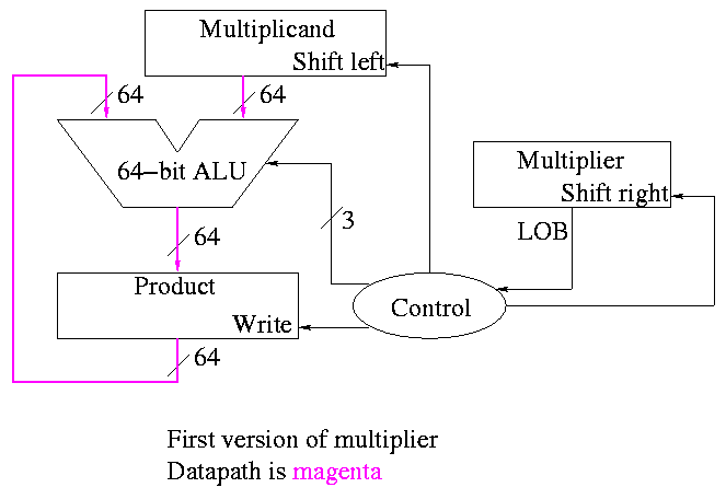
What about the control?
-
Always give the ALU the ADD operation
-
Always send a 1 to the multiplicand to shift left
-
Always send a 1 to the multiplier to shift right
-
Pretty boring so far but
-
Send a 1 to write line in product if and only if
LOB multiplier is a 1
-
I.e. send LOB to write line
-
I.e. it really is pretty boring
This works!
But, when compared to the better solutions to come, is wasteful of
resourses and hence is
-
slower
-
hotter
-
bigger
-
all these are bad
The product register must be 64 bits since the product can contain 64
bits.
Why is multiplicand register 64 bits?
-
So that we can shift it left
-
I.e., for our convenience.
By this I mean it is not required by the problem specification,
but only by the solution method chosen.
Why is ALU 64-bits?
-
Because the product is 64 bits
-
But we are only adding a 32-bit quantity to the
product at any one step.
-
Hmmm.
-
Maybe we can just pull out the correct bits from the product.
-
Would be tricky to pull out bits in the middle
because which bits to pull changes each step
POOF!! ... as the smoke clears we see an idea.
We can solve both problems at once
-
DON'T shift the multiplicand left
-
Hence register is 32-bits.
-
Also register need not be a shifter
-
Instead shift the product right!
-
Add the high-order (HO) 32-bits of product register to the
multiplicand and place the result back into HO 32-bits
-
Only do this if the current multiplier bit is one.
-
Use the Carry Out of the sum as the new bit to shift
in
-
The book forgot the last point but their example used numbers
too small to generate a carry
This results in the following algorithm
    product <- 0
    for i = 0 to 31
        if LOB of multiplier = 1
            (serial_in, product[32-63]) <- product[32-63] + multiplicand
        shift product right 1 bit
        shift multiplier right 1 bit
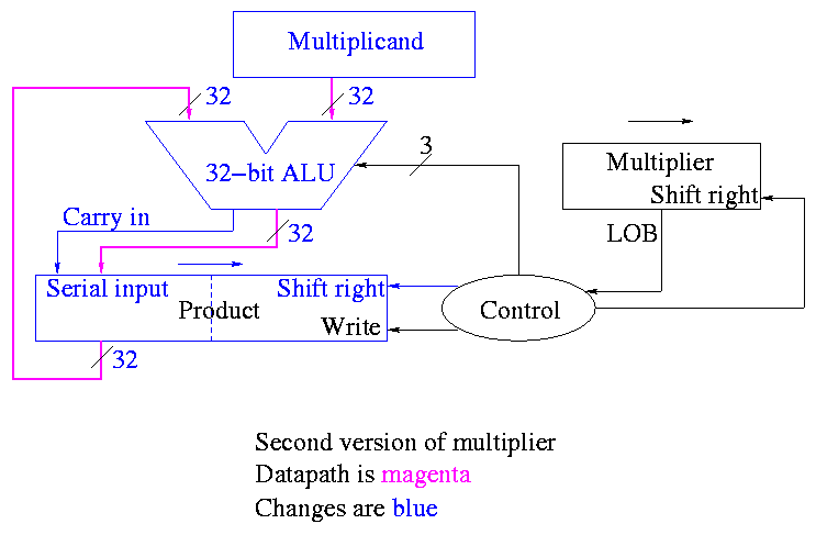
What about control
-
Just as boring as before
-
Send (ADD, 1, 1) to (ALU, multiplier (shift right), Product
(shift right)).
-
Send LOB to Product (write).
Redo same example on board
A final trick (``gate bumming'', like code bumming of 60s).
-
There is a waste of registers, i.e. not full unilization.
-
The multiplicand is fully unilized since we always need all 32 bits.
-
But once we use a multiplier bit, we can toss it so we need
less and less of the multiplier as we go along.
-
And the product is half unused at beginning and only slowly ...
-
POOF!!
-
``Timeshare'' the LO half of the ``product register''.
-
In the beginning LO half contains the multiplier.
-
Each step we shift right and more goes to product
less to multiplier.
-
The algorithm changes to:
    product[0-31] <- multiplier
    for i = 0 to 31
        if LOB of product = 1
            (serial_in, product[32-63]) <- product[32-63] + multiplicand
        shift product right 1 bit
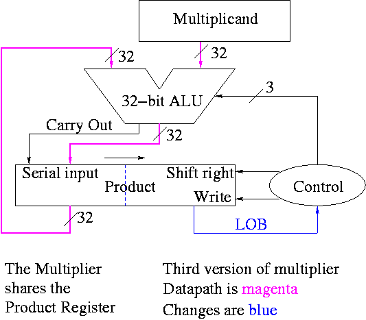
Control again boring.
- Send (ADD, 1) to (ALU, Product (shift right)).
- Send LOB to Product (write).
Redo the same example on the board.
The above was for unsigned 32-bit multiplication.
What about signed multiplication.
-
Save the signs of the multiplier and multiplicand.
-
Convert multiplier and multiplicand to non-neg numbers.
-
Use above algorithm.
-
Only use 31 steps not 32 since there are only 31 multiplier bits
(the HOB of the multiplier is the sign bit, not a bit used for
multiplying).
-
Compliment product if original signs were different.
There are faster multipliers, but we are not covering them.
4.7: Division
We are skiping division.
4.8: Floating Point
We are skiping floating point.
4.9: Real Stuff: Floating Point in the PowerPC and 80x86
We are skiping floating point.
Homework:
Read 4.10 ``Fallacies and Pitfalls'', 4.11 ``Conclusion'',
and 4.12 ``Historical Perspective''.
======== START LECTURE #12
========
Notes:
Midterm exam 25 Oct.
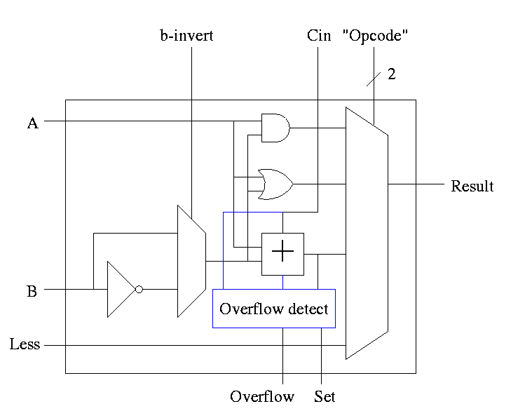
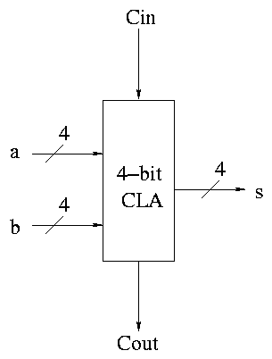
Lab 2. Due 1 November. Extend Modify lab 1 to a 32 bit alu that
in addition handles sub, slt, zero detect, and overflow. That is,
produce a gate level simulation of Figure 4.19. This figure is also
in the class notes; it is the penultimate figure before ``Fast Adders''.
It is NOW DEFINITE that on monday 23 Oct, my office
hours will have to move from 2:30--3:30 to 1:30-2:30 due to a
departmental committee meeting.
Don't forget the mirror site. My main website will be
going down for an OS upgrade at some point. Start at http://cs.nyu.edu
End of Notes:
Chapter 5: The processor: datapath and control
Homework:
Start Reading Chapter 5.
5.1: Introduction
We are going to build the MIPS processor
Figure 5.1 redrawn below shows the main idea
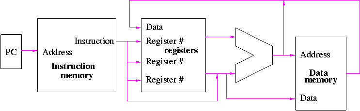
Note that the instruction gives the three register numbers as well
as an immediate value to be added.
- No instruction actually does all this.
- We have datapaths for all possibilities.
- Will see how we arrange for only certain datapaths to be used for
each instruction type.
- For example R type uses all three registers but not the
immediate field.
- The I type uses the immediate but not all three registers.
- The memory address for a load or store is the sum of a register
and an immediate.
- The data value to be stored comes from a register.
5.2: Building a datapath
Let's begin doing the pieces in more detail.
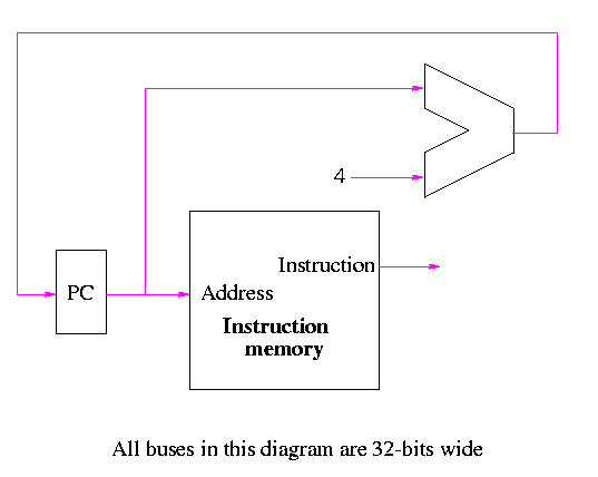
Instruction fetch
We are ignoring branches for now.
- How come no write line for the PC register?
- Ans: We write it every cycle.
- How come no control for the ALU
- Ans: This one always adds
R-type instructions
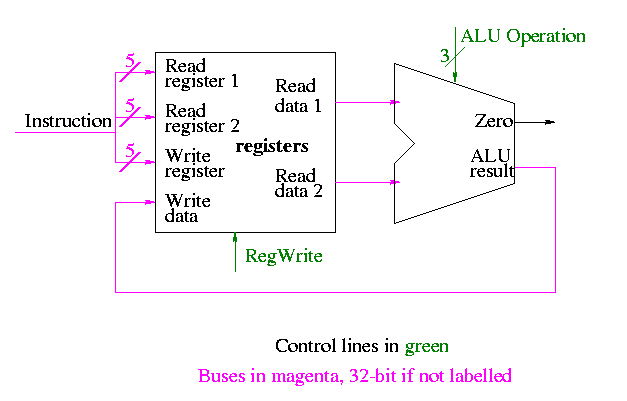
- ``Read'' and ``Write'' in the diagram are adjectives not verbs.
- The 32-bit bus with the instruction is divided into three 5-bit
buses for each register number (plus other wires not shown).
- Two read ports and one write port, just as we learned in chapter 4.
- The 3-bit control consists of Bnegate and Op from chapter 4.
- The RegWrite control line is always asserted for R-type
instructions.
Homework: What would happen if the RegWrite line
had a stuck-at-0 fault (was always deasserted)?
What would happen if the RegWrite line
had a stuck-at-1 fault (was always asserted)?
load and store
lw  $r,disp($s)
sw  $r,disp($s)
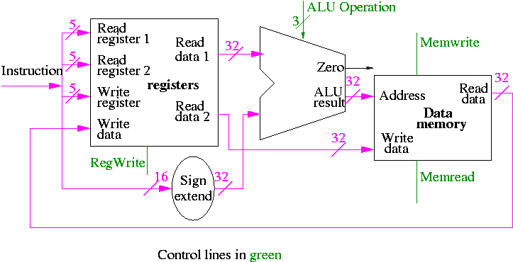
- lw $r,disp($s):
- Computes the effective address formed by adding the 16-bit
immediate constant ``disp'' to the contents of register $s.
- Fetches the value in data memory at this address.
- Inserts this value into register $r.
- sw $r,disp($s):
- Computes the same effective address as lw $r,disp($s)
- Stores the contents of register $r into this address
- We have a 32-bit adder so need to extend the 16-bit immediate
constant to 32 bits. Produce an additional 16 HOBs all equal to the
sign bit of the 16-bit immediate constant. This is called sign
extending the constant.
- RegWrite is deasserted for sw and asserted for lw.
- MemWrite is asserted for sw and deasserted for lw.
- I don't see the need for MemRead; perhaps it is there for power
saving.
- The ALU Operation is set to add for lw and sw.
- For now we just write down which control lines are asserted and
deasserted. Later we will do the circuit for to calculate the control
lines from the instruction word.
Homework: What would happen if the RegWrite line
had a stuck-at-0 fault (was always deasserted)?
What would happen if the RegWrite line
had a stuck-at-1 fault (was always asserted)?
What would happen if the MemWrite line
had a stuck-at-0 fault (was always deasserted)?
What would happen if the MemWrite line
had a stuck-at-1 fault (was always asserted)?
There is a cheat here.
- For lw we read register r (and read s)
- For sw we write register r (and read s)
- But we indicated that the same bits in the instruction always go to
the same ports in the register file.
- We are ``mux deficient''.
- We will put in the mux later
Branch on equal (beq)
Compare two registers and branch if equal.
- To check for equal we subtract and test for zero (our ALU does
this).
- If $r=$s, the target of the branch beq $r,$s,disp is the sum of
- The program counter PC after it has been incremented,
that is the address of the next sequential instruction
- The 16-bit immediate constant ``disp'' (treated as a signed
number) left shifted 2 bits.
- The value of PC after the increment is available. We computed it
in the basic instruction fetch datapath.
- Since the immediate constant is signed it must be sign extended.
Homework: What would happen if the RegWrite line
had a stuck-at-0 fault (was always deasserted)?
What would happen if the RegWrite line
had a stuck-at-1 fault (was always asserted)?
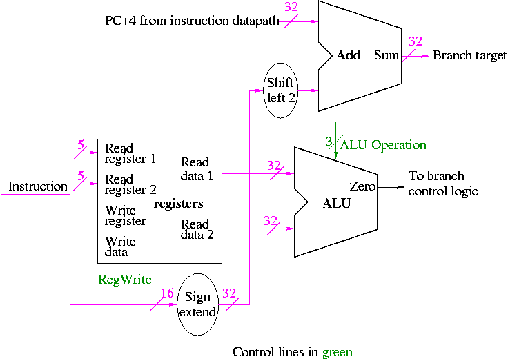
- The top ``alu symbol'' labeled ``add'' is just an adder so does
not need any control
- The shift left 2 is not a shifter. It simply moves wires and
includes two zero wires. We need a 32-bit version. Below is a 5 bit
version.
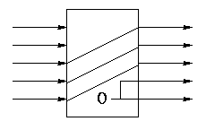
5.3: A simple implementation scheme
We will just put the pieces together and then figure out the control
lines that are needed and how to set them. We are not now worried
about speed.
We are assuming that the instruction memory and data memory are
separate. So we are not permitting self modifying code. We are not
showing how either memory is connected to the outside world (i.e. we
are ignoring I/O).
We have to use the same register file with all the pieces since when a
load changes a register a subsequent R-type instruction must see the
change, when an R-type instruction makes a change the lw/sw must see
it (for loading or calculating the effective address, etc.
We could use separate ALUs for each type but it is easy not to so we
will use the same ALU for all. We do have a separate adder for
incrementing the PC.
Combining R-type and lw/sw
The problem is that some inputs can come from different sources.
- For R-type, both ALU operands are registers. For I-type (lw/sw)
the second operand is the (sign extended) immediate field.
- For R-type, the write data comes from the ALU. For lw it comes
from the memory.
- For R-type, the write register comes from field rd, which is bits
15-11. For sw, the write register comes from field rt, which is bits
20-16.
We will deal with the first two now by using a mux for each. We
will deal with the third shortly by (surprise) using a mux.
Combining R-type and lw/sw
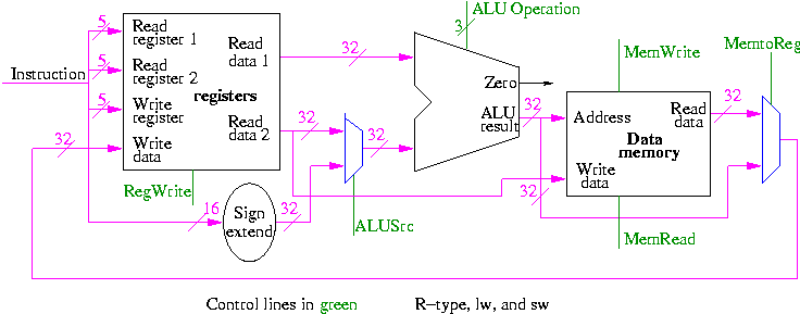
======== START LECTURE #13
========
Including instruction fetch
This is quite easy
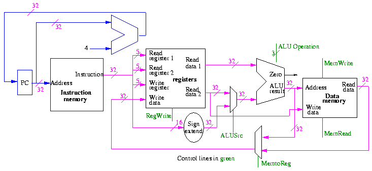
Finally, beq
We need to have an ``if stmt'' for PC (i.e., a mux)
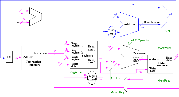
Homework: 5.5 (just the datapath, not the control),
5.8 (just the datapath, not the control), 5.9.
The control for the datapath
We start with our last figure, which shows the data path and then add
the missing mux and show how the instruction is broken down.

We need to set the muxes.
We need to generate the three ALU cntl lines: 1-bit Bnegate and 2-bit OP
    And     0 00
    Or      0 01
    Add     0 10
    Sub     1 10
    Set-LT  1 11
Homework:
What happens if we use 1 00 for the three ALU control lines?
What if we use 1 01?
What information can we use to decide on the muxes and alu cntl lines?
The instruction!
-
Opcode field (6 bits)
-
For R-type the funct field (6 bits)
So no problem, just do a truth table.
-
12 inputs, 3 outputs (this is just for the three ALU control lines).
-
4096 rows, 15 columns, 60K entries
-
HELP!
We will let the main control (to be done later) ``summarize''
the opcode for us. It will generate a 2-bit field ALUOp
    ALUOp   Action needed by ALU

    00      Addition (for load and store)
    01      Subtraction (for beq)
    10      Determined by funct field (R-type instruction)
    11      Not used
How many entries do we have now in the truth table?
-
Instead of a 6-bit opcode we have a 2-bit summary.
-
We still have a 6-bit function (funct) field (needed for R-type).
-
So now we have 8 inputs (2+6) and 3 outputs.
-
256 rows, 11 columns; ~2800 entries.
-
Certainly easy for automation ... but we will be clever.
-
We only have 8 MIPS instructions that use the ALU (fig 5.15).
| opcode |
ALUOp |
operation |
funct field |
ALU action |
ALU cntl |
| LW |
00 |
load word |
xxxxxx |
add |
010 |
| SW |
00 |
store word |
xxxxxx |
add |
010 |
| BEQ |
01 |
branch equal |
xxxxxx |
subtract |
110 |
| R-type |
10 |
add |
100000 |
add |
010 |
| R-type |
10 |
subtract |
100010 |
subtract |
110 |
| R-type |
10 |
AND |
100100 |
and |
000 |
| R-type |
10 |
OR |
100101 |
or |
001 |
| R-type |
10 |
SLT |
101010 |
set on less than |
111 |
-
The first two rows are the same
-
When funct is used its two HOBs are 10 so are don't care
-
ALUOp=11 impossible ==> 01 = X1 and 10 = 1X
-
So we get
    ALUOp | Funct        ||  Bnegate:OP
    1 0   | 5 4 3 2 1 0  ||  B OP
    ------+--------------++------------
    0 0   | x x x x x x  ||  0 10
    x 1   | x x x x x x  ||  1 10
    1 x   | x x 0 0 0 0  ||  0 10
    1 x   | x x 0 0 1 0  ||  1 10
    1 x   | x x 0 1 0 0  ||  0 00
    1 x   | x x 0 1 0 1  ||  0 01
    1 x   | x x 1 0 1 0  ||  1 11
- How would we implement this?
- A circuit for each of the three output bits.
- Must decide when each output bit is 1.
- We do this one output bit at a time.
- When is Bnegate (called Op2 in book) asserted?
- When is OP1 asserted?
- Again we begin with the rows where its bit is one
    ALUOp | Funct
    1 0   | 5 4 3 2 1 0
    ------+------------
    0 0   | x x x x x x
    x 1   | x x x x x x
    1 x   | x x 0 0 0 0
    1 x   | x x 0 0 1 0
    1 x   | x x 1 0 1 0
- Again inspection of the 5 rows with ALUOp=1x yields one F bit that
distinguishes when OP1 is asserted, namely F2=0
    ALUOp | Funct
    1 0   | 5 4 3 2 1 0
    ------+------------
    0 0   | x x x x x x
    x 1   | x x x x x x
    1 x   | x x x 0 x x
- Since x 1 in the second row is really 0 1, rows 1 and 2
can be combined to give
    ALUOp | Funct
    1 0   | 5 4 3 2 1 0
    ------+------------
    0 x   | x x x x x x
    1 x   | x x x 0 x x
- Now we can use the first row to enlarge the scope of the
last row
    ALUOp | Funct
    1 0   | 5 4 3 2 1 0
    ------+------------
    0 x   | x x x x x x
    x x   | x x x 0 x x
- So OP1 = NOT ALUOp1 + NOT F2
- When is OP0 asserted?
The circuit is then easy.
======== START LECTURE #14
========
Now we need the main control.
-
setting the four muxes.
-
Writing the registers.
-
Writing the memory.
-
Reading the memory (for technical reasons, would not be needed if
the memory was built from registers).
-
Calculating ALUOp.
So 9 bits.
The following figure shows where these occur.
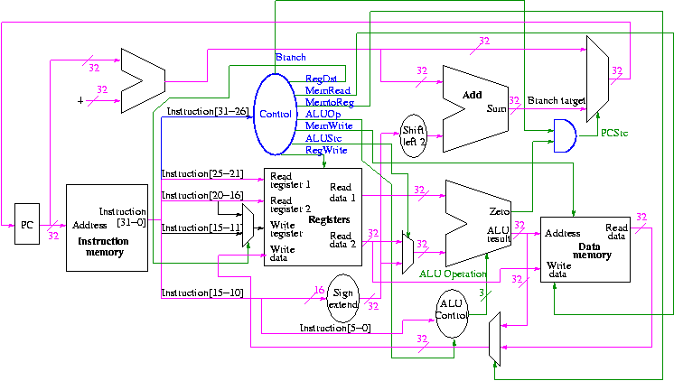
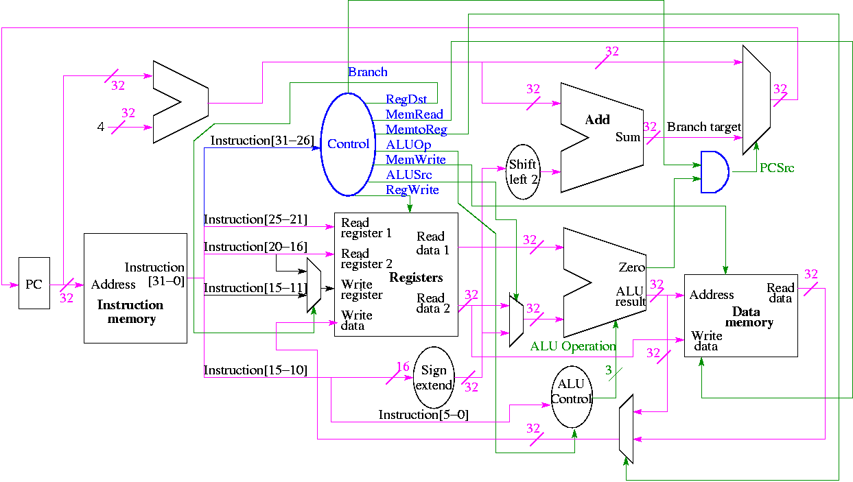
They all are determined by the opcode
The MIPS instruction set is fairly regular. Most fields we need
are always in the same place in the instruction.
-
Opcode (called Op[5-0]) is always in 31-26
-
Regs to be read always 25-21 and 20-16 (R-type, beq, store)
-
Base reg for effective address always 25-21 (load store)
-
Offset always 15-0
-
Oops: Reg to be written EITHER 20-16 (load) OR 15-11 (R-type) MUX!!
| MemRead: |
Memory delivers the value stored at the specified addr |
| MemWrite: |
Memory stores the specified value at the specified addr |
| ALUSrc: |
Second ALU operand comes from (reg-file / sign-ext-immediate) |
| RegDst: |
Number of reg to write comes from the (rt / rd) field |
| RegWrite: |
Reg-file stores the specified value in the specified register |
| PCSrc: |
New PC is Old PC+4 / Branch target |
| MemtoReg: |
Value written in reg-file comes from (alu / mem) |
We have seen the wiring before (and have a hardcopy to handout).
We are interested in four opcodes.
Do a stage play
- Need ``volunteers''
- One for each of 4 muxes
- One for PC reg
- One for the register file
- One for the instruction memory
- One for the data memory
- I will play the control
- Let the PC initially be zero
- Let each register initially contain its number (e.g. R2=2)
- Let each data memory word initially contain 100 times its address
- Let the instruction memory contain (starting at zero)
add r9,r5,r1 r9=r5+r1   0   5   1   9   0  32
sub r9,r9,r6            0   9   6   9   0  34
beq r9,r0,-8            4   9   0   <  -2   >
slt r1,r9,r0            0   9   0   1   0  42
lw  r1,102(r2)         35   2   1   <  100  >
sw  r9,102(r2)
- Go!
The following figures illustrate the play.
We start with R-type instructions

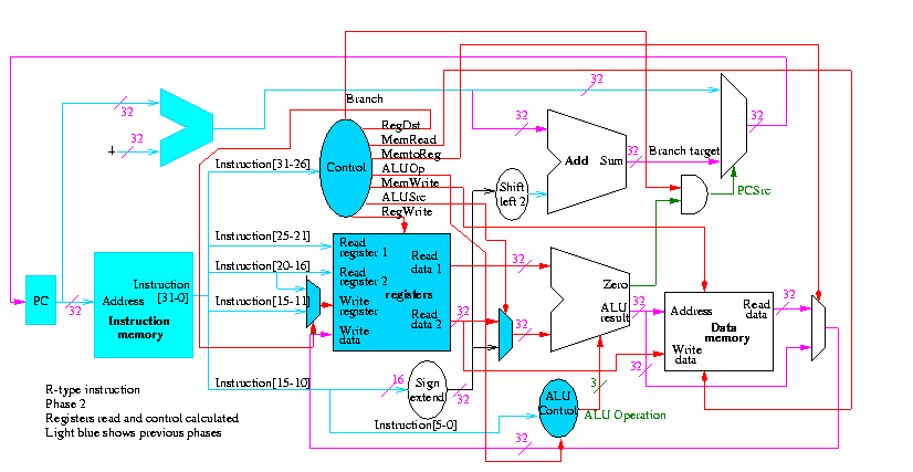
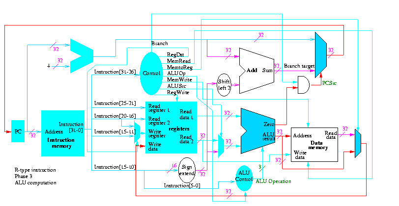
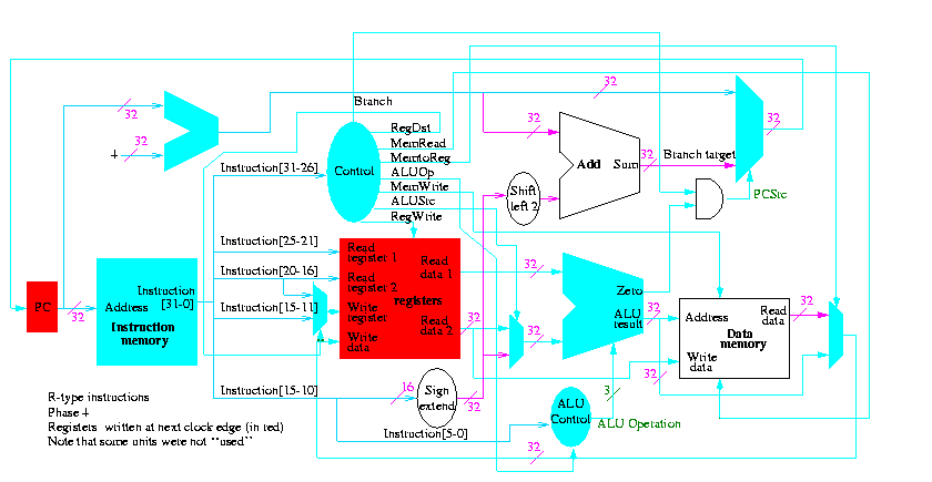
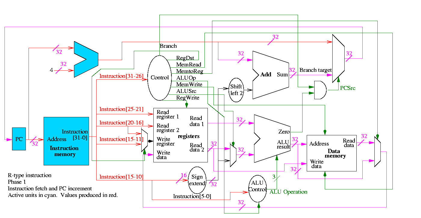
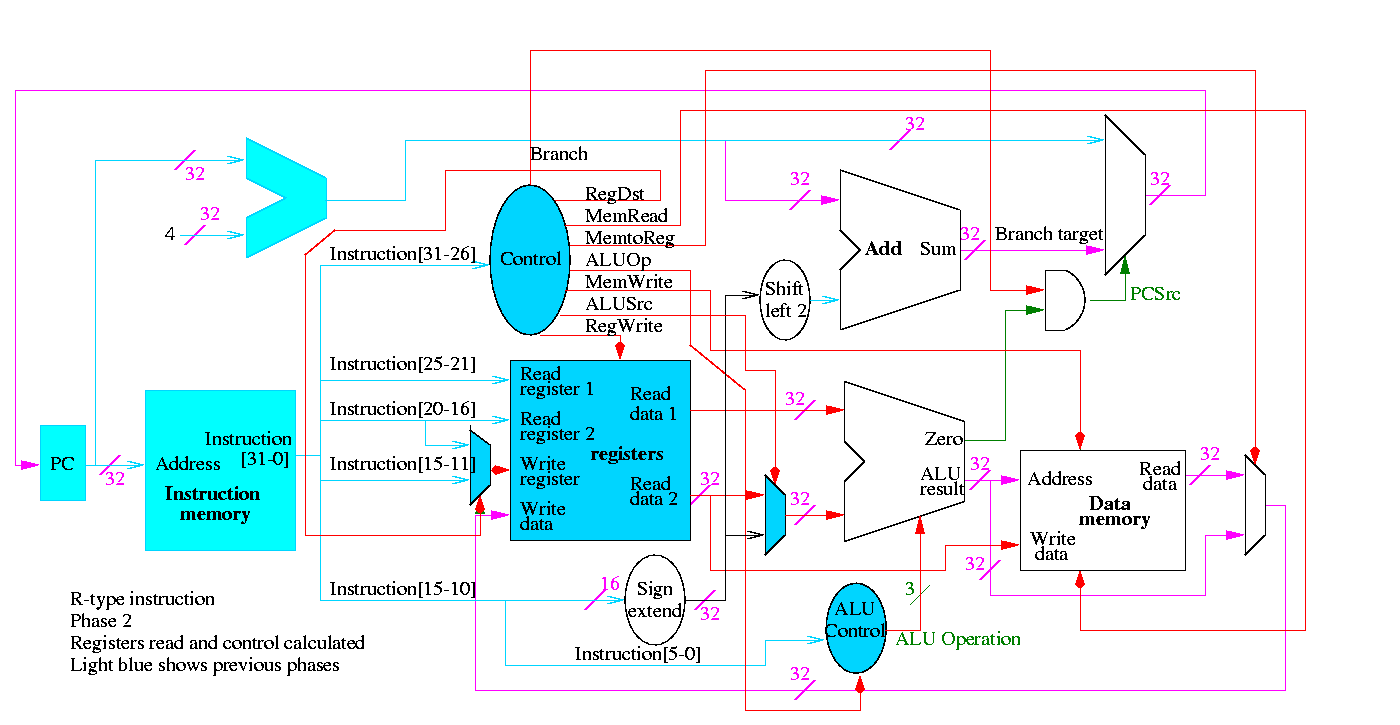
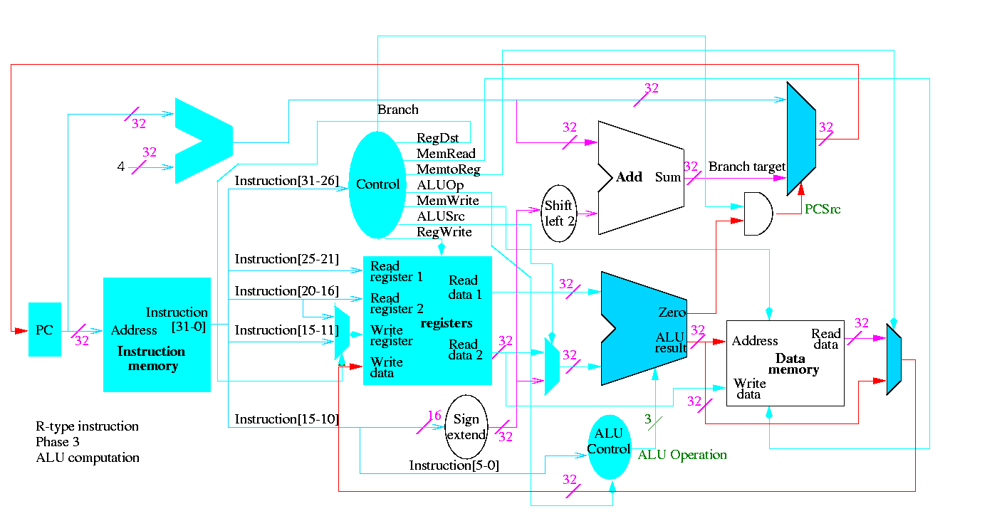
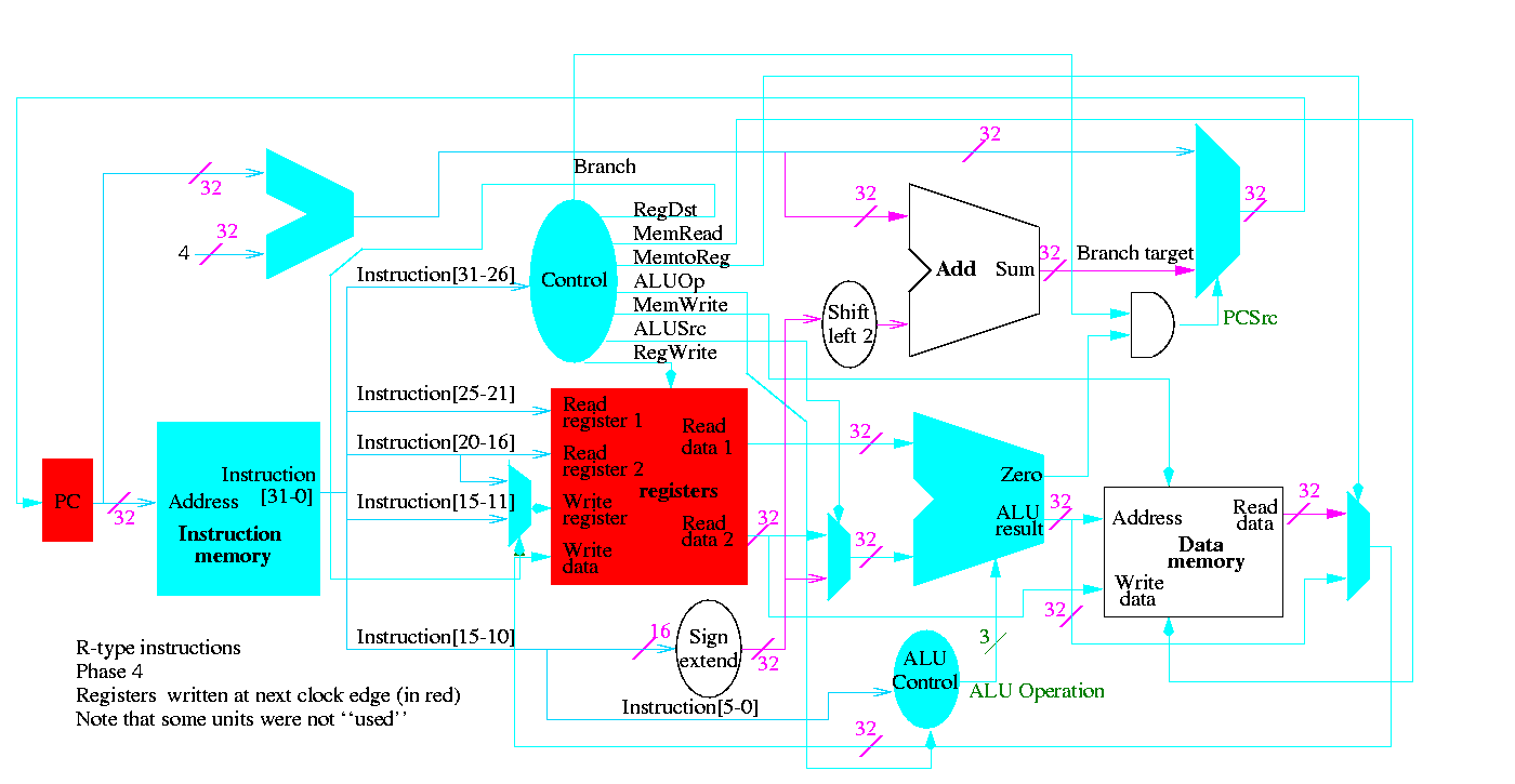
Next we show lw
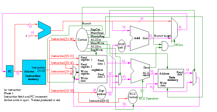
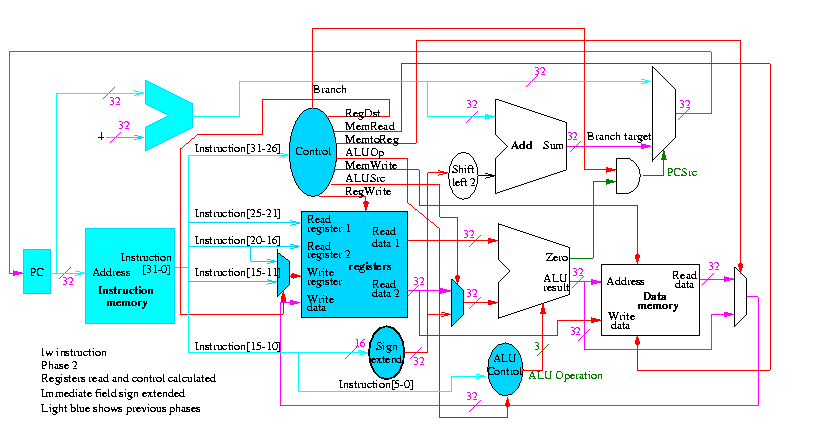

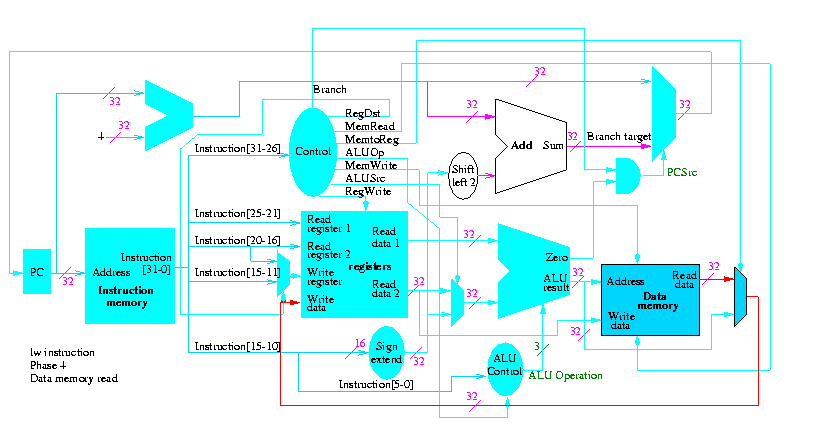
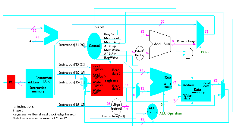


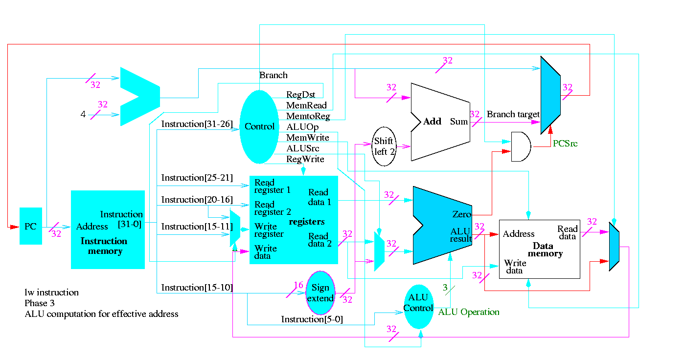
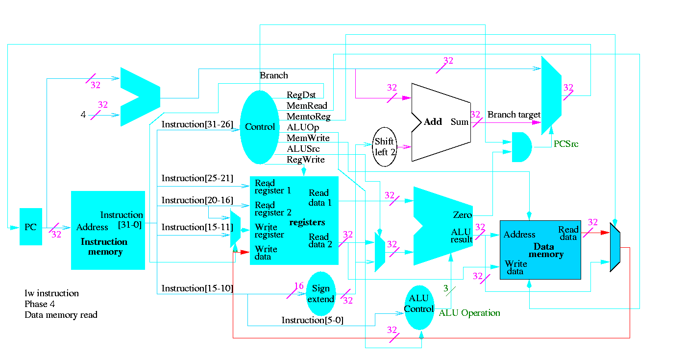

The following truth table shows the settings for the control lines for
each opcode. This is drawn differently since the labels of what
should be the columns are long (e.g. RegWrite) and it is easier to
have long labels for rows.
| Signal | R-type | lw | sw | beq |
| Op5 | 0 | 1 | 1 | 0 |
| Op4 | 0 | 0 | 0 | 0 |
| Op3 | 0 | 0 | 1 | 0 |
| Op2 | 0 | 0 | 0 | 1 |
| Op1 | 0 | 1 | 1 | 0 |
| Op0 | 0 | 1 | 1 | 0 |
| RegDst | 1 | 0 | X | X |
| ALUSrc | 0 | 1 | 1 | 0 |
| MemtoReg | 0 | 1 | X | X |
| RegWrite | 1 | 1 | 0 | 0 |
| MemRead | 0 | 1 | 0 | 0 |
| MemWrite | 0 | 0 | 1 | 0 |
| Branch | 0 | 0 | 0 | 1 |
| ALUOp1 | 1 | 0 | 0 | 0 |
| ALUOp | 0 | 0 | 0 | 1 |
Now it is straightforward but tedious to get the logic equations
When drawn in pla style the circuit is
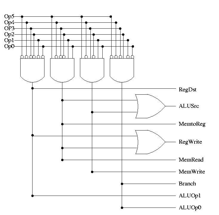
======== START LECTURE #15
========
Midterm Exam
======== START LECTURE #16
========
Notes:
I might have said that for simulating NOT in the lab ~ was good and !
is bad.
That is wrong.
You SHOULD use !x for (NOT x).
The problem with ~ is that
~1 isn't zero, i.e. ~ TRUE is still TRUE.
The class did well on the midterm.
Although the exam was not very difficult, I am delighted the class did
well.
The only bad part is that the few students who did not do well need to
study more as the final certainly won't be easier.
I will go over the exam in a few minutes when more
students have arrived.
The median grade was 87 and the breakdown was
90-100 18
80-89  14
70-79   8
60-69   2
50-59   1
Lab2 is due on Wednesday
End of Notes.
Homework:
5.5 and 5.8 (control, we already did the datapath), 5.1, 5.2, 5.10
(just the single-cycle datapath) 5.11.
Implementing a J-type instruction, unconditional jump
    opcode  addr
    31-26   25-0
Addr is word address; bottom 2 bits of PC are always 0
Top 4 bits of PC stay as they were (AFTER incr by 4)
Easy to add.

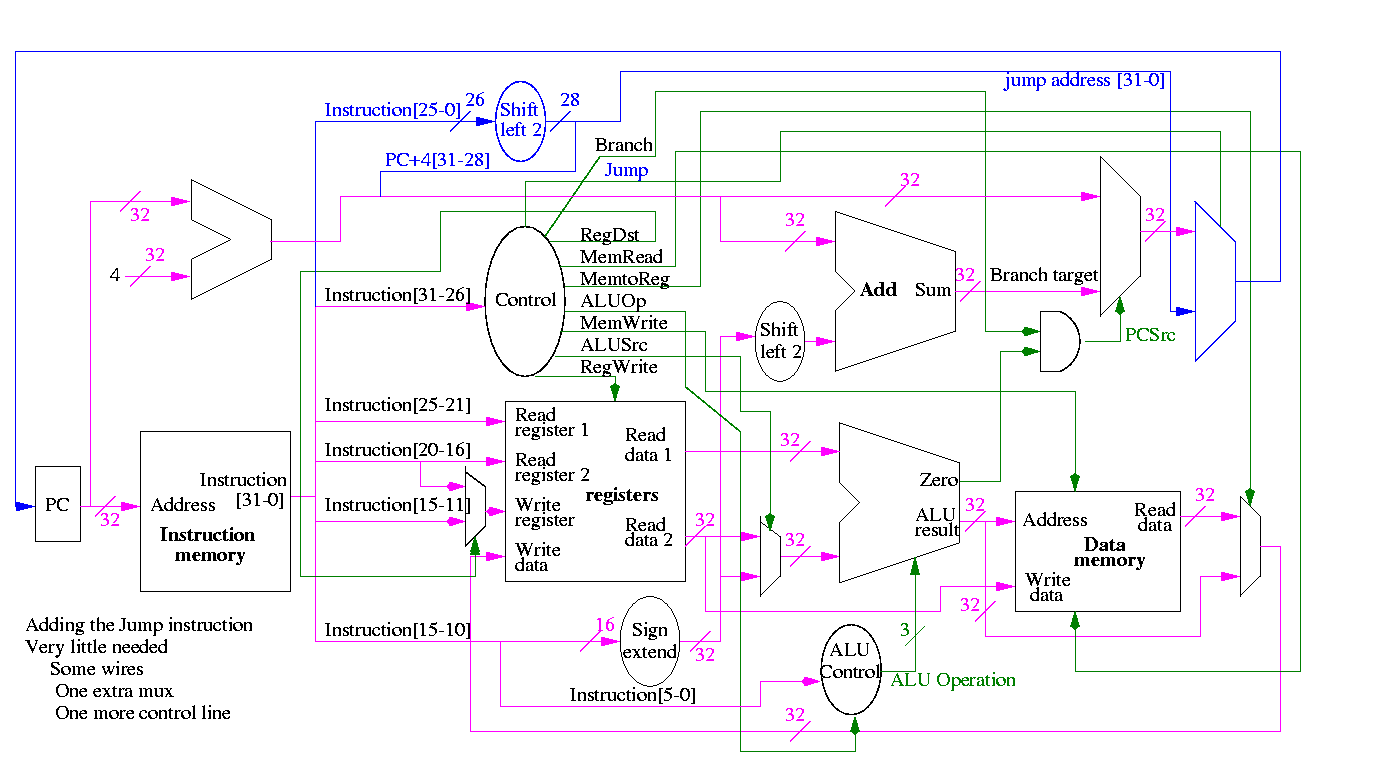
Smells like a good final exam type question.
What's Wrong
Some instructions are likely slower than others and we must set the
clock cycle time long enough for the slowest. The disparity between
the cycle times needed for different instructions is quite significant
when one considers implementing more difficult instructions, like
divide and floating point ops. Actually, if we considered cache
misses, which result in references to external DRAM, the cycle time
ratios can approach 100.
Possible solutions
-
Variable length cycle. How do we do it?
-
Asynchronous logic
-
``Self-timed'' logic.
-
No clock. Instead each signal (or group of signals) is
coupled with another signal that changes only when the first
signal (or group) is stable.
-
Hard to debug.
-
Multicycle instructions.
-
More complicated instructions have more cycles.
-
Since only one instruction is executed at a time, can reuse a
single ALU and other resourses during different cycles.
-
It is in the book right at this point but we are not covering it.
======== START LECTURE #17
========
Note:
Lab 3 (the final lab) handed out today due 20 November.
Even Faster (we are not covering this).
-
Pipeline the cycles.
-
Since at one time we will have several instructions active, each
at a different cycle, the resourses can't be reused (e.g., more
than one instruction might need to do a register read/write at one
time).
-
Pipelining is more complicated than the single cycle
implementation we did.
-
This was the basic RISC technology on the 1980s.
-
A pipelined implementation of the MIPS CPU is covered in chapter 6.
-
Multiple datapaths (superscalar).
-
Issue several instructions each cycle and the hardware
figures out dependencies and only executes instructions when the
dependencies are satisfied.
-
Much more logic required, but conceptually not too difficult
providing the system executes instructions in order.
-
Pretty hairy if out of order (OOO) exectuion is
permitted.
-
Current high end processors are all OOO superscalar (and are
indeed pretty hairy).
-
VLIW (Very Long Instruction Word)
-
User (i.e., the compiler) packs several instructions into one
``superinstruction'' called a very long instruction.
-
User guarentees that there are no dependencies within a
superinstruction.
-
Hardware still needs multiple datapaths (indeed the datapaths are
not so different from superscalar).
-
The hairy control for superscalar (especially OOO superscalar)
is not needed since the dependency
checking is done by the compiler, not the hardware.
-
Was proposed and tried in 80s, but was dominated by superscalar.
-
A comeback (?) with Intel's EPIC (Explicitly Parallel Instruction
Computer) architecture.
-
Called IA-64 (Intel Architecture 64-bits); the first
implementation was called Merced and now has a funny name
(Itanium). It should be available RSN (Real Soon Now).
-
It has other features as well (e.g. predication).
-
The x86, Pentium, etc are called IA-32.
Chapter 2 Performance analysis
Homework:
Read Chapter 2
2.1: Introductions
Throughput measures the number of jobs per day
that can be accomplished. Response time measures how
long an individual job takes.
- A faster machine improves both metrics (increases throughput and
decreases response time).
- Normally anything that improves response time improves throughput.
- But the reverse isn't true. For example,
adding a processor likely to increase throughput more than
it decreases response time.
-
We will be concerned primarily with response time.
We define Performance as 1 / Execution time.
So machine X is n times faster than Y means that
-
The performance of X = n * the performance of Y.
-
The execution time of X = (1/n) * the execution time of Y.
2.2: Measuring Performance
How should we measure execution time?
-
CPU time.
-
This includes the time waiting for memory.
-
It does not include the time waiting for I/O
as this process is not running and hence using no CPU time.
-
Elapsed time on an otherwise empty system.
-
Elapsed time on a ``normally loaded'' system.
-
Elapsed time on a ``heavily loaded'' system.
We use CPU time, but this does not mean the other
metrics are worse.
Cycle time vs. Clock rate.
- Recall that cycle time is the length of a cycle.
- It is a unit of time.
- For modern computers it is expressed in nanoseconds,
abbreviated ns.
- One nanosecond is one billionth of a second = 10^(-9) seconds.
- Electricity travels about 1 foot in 1ns (in normal media).
- The clock rate tells how many cycles fit into a given time unit
(normally in one second).
- So the natural unit for clock rate is cycles per second.
This used to be abbreviated CPS.
- However, the world has changed and the new name for the same
thing is Hertz, abbreviated Hz.
One Hertz is one cycle per second.
- For modern computers the rate is expressed in megahertz,
abbreviated MHz.
- One megahertz is one million hertz = 10^6 hertz.
- A few machines have a clock rate exceeding a gigahertz (GHz).
Next year many new machines will pass the gigahertz mark;
possibly some will exceed 2GHz.
- One gigahertz is one billion hertz = 10^9 hertz.
- What is the cycle time for a 700MHz computer?
- 700 million cycles = 1 second
- 7*10^8 cycles = 1 second
- 1 cycle = 1/(7*10^8) seconds = 10/7 * 10^(-9) seconds ~= 1.4ns
- What is the clock rate for a machine with a 10ns cycle time?
- 1 cycle = 10ns = 10^(-8) seconds.
- 10^8 cycles = 1 second.
- Rate is 10^8 Hertz = 100 * 10^6 Hz = 100MHz = 0.1GHz
2.3: Relating the metrics
The execution time for a given job on a given computer is
(CPU) execution time = (#CPU clock cycles required) * (cycle time)
                     = (#CPU clock cycles required) / (clock rate)
The number of CPU clock cycles required equals the number of
instructions executed times the number of cycles in each
instruction.
- In our single cycle implementation, the number of cycles required
is just the number of instructions executed.
- If every instruction took 5 cycles, the number of cycles required
would be five times the number of instructions executed.
But real systems are more complicated than that!
- Some instructions take more cycles than others.
- With pipelining, several instructions are in progress at different
stages of their execution.
- With super scalar (or VLIW) many instructions are issued at once.
- Since modern superscalars (and VLIWs) are also pipelined we have
many many instructions executing at once.
Through a great many measurement, one calculates for a given machine
the average CPI (cycles per instruction).
The number of instructions required for a given program depends on
the instruction set.
For example, we saw in chapter 3 that 1 Vax instruction is often
accomplishes more than 1 MIPS instruction.
Complicated instructions take longer; either more cycles or longer cycle
time.
Older machines with complicated instructions (e.g. VAX in 80s) had CPI>>1.
With pipelining can have many cycles for each instruction but still
have CPI nearly 1.
Modern superscalar machines have CPI < 1.
-
They issue many instructions each cycle.
-
They are pipelined so the instructions don't finish for several cycles.
-
If we consider a 4-issue superscalar and assume that all
instructions require 5 (pipelined) cycles, there are
up to 20=5*4 instructions in progress (often called in flight) at
one time.
Putting this together, we see that
   Time (in seconds) =  #Instructions * CPI * Cycle_time (in seconds).
   Time (in ns)      =  #Instructions * CPI * Cycle_time (in ns).
Homework:
Carefully go through and understand the example on page 59
Homework:
2.1-2.5 2.7-2.10
Homework:
Make sure you can easily do all the problems with a rating of
[5] and can do all with a rating of [10]
======== START LECTURE #18
========
What is the MIPS rating for a computer and how useful is it?
-
MIPS stands for Millions of Instructions Per Second.
- It is a unit of rate or speed (like MHz), not of time (like ns.).
-
It is not the same as the MIPS computer (but the name
similarity is not a coincidence).
- The number of seconds required to execute a given (machine
language) program is
the number of instructions executed / the number executed per second.
- The number of microseconds required to execute a given (machine
language) program is
the number of instructions executed / MIPS.
-
BUT ... .
- The same program in C (or Java, or Ada, etc) might need
different number of instructions
on different computers.
For example, one VAX instruction might require 2
instructions on a power-PC and 3 instructions on an X86).
- The same program in C when compiled by two different compilers
for the same computer architecture, might need to executed
different numbers of instructions.
-
Different programs may achieve different MIPS ratings on the
same architecture.
- Some programs execute more long instructions
than do other programs.
- Some programs have more cache misses and hence cause
more waiting for memory.
- Some programs inhibit full pipelining
(e.g., they may have more mispredicted branches).
- Some programs inhibit full superscalar behavior
(e.g., they may have unhideable data dependencies).
-
One can often raise the MIPS rating by adding NOPs, despite
increasing execution time. How?
Ans. MIPS doesn't require useful instructions and
NOPs, while perhaps useless, are nonetheless very fast.
- So, unlike MHz, MIPS is not a value that be defined for a specific
computer; it depends on other factors, e.g., language/compiler used,
problem solved, and algorithm employed.
Homework:
Carefully go through and understand the example on pages 61-3
How about MFLOPS (Million of FLoating point OPerations per Second)?
For numerical calculations floating point operations are the
ones you are interested in; the others are ``overhead'' (a
very rough approximation to reality).
It has similar problems to MIPS.
- The same program needs different numbers of floating point operations
on different machines (e.g., is sqrt one instruction or several?).
- Compilers effect the MFLOPS rating.
- MFLOPS is Not as bad as MIPS since adding NOPs lowers the MFLOPs
rating.
- But you can insert unnecessary floating point ADD instructions
and this will probably raise the MFLOPS rating. Why?
Because it will lower the percentage of ``overhead'' (i.e.,
non-floating point) instructions.
Benchmarks are better than MIPS or MFLOPS, but still have difficulties.
- It is hard to find benchmarks that represent your future
usage.
- Compilers can be ``tuned'' for important benchmarks.
- Benchmarks can be chosen to favor certain architectures.
- If your processor has 256KB of cache memory and
your competitor's has 128MB, you try to find a benchmark that
frequently accesses a region of memory having size between 128MB
and 256MB.
- If your 128MB cache is 2 way set associative (defined later this
month) while your competitors 256MB cache is direct mapped, then
you build/choose a benchmark that frequently accesses exactly two
10K arrays separated by an exact multiple of 256KB.
Homework:
Carefully go through and understand 2.7 ``fallacies and pitfalls''.
Chapter 7: Memory
Homework:
Read Chapter 7
7.2: Introduction
Ideal memory is
-
Big (in capacity; not physical size).
-
Fast.
-
Cheap.
-
Impossible.
So we use a memory hierarchy ...
-
Registers
-
Cache (really L1, L2, and maybe L3)
-
Memory
-
Disk
-
Archive
... and try to catch most references
in the small fast memories near the top of the hierarchy.
There is a capacity/performance/price gap between each pair of
adjacent levels.
We will study the cache <---> memory gap
-
In modern systems there are many levels of caches.
-
Similar considerations apply to the other gaps (e.g.,
memory<--->disk, where virtual memory techniques are applied).
This is the gap studied in 202.
-
But the terminology is often different, e.g., in architecture we
evict cache blocks or lines whereas in OS we evict pages.
-
In fall 97 my OS class was studying ``the same thing'' at this
exact point (memory management). That isn't true this year since
the OS text changed and memory management is earlier.
We observe empirically (and teach in 202).
-
Temporal Locality: The word referenced now is likely to be
referenced again soon. Hence it is wise to keep the currently
accessed word handy (high in the memory hierarchy) for a while.
-
Spatial Locality: Words near the currently referenced
word are likely to be referenced soon. Hence it is wise to
prefetch words near the currently referenced word and keep them
handy (high in the memory hierarchy) for a while.
A cache is a small fast memory between the
processor and the main memory. It contains a subset of the contents
of the main memory.
A Cache is organized in units of blocks.
Common block sizes are 16, 32, and 64 bytes.
This is the smallest unit we can move to/from a cache.
-
We view memory as organized in blocks as well. If the block
size is 16, then bytes 0-15 of memory are in block 0, bytes 16-31
are in block 1, etc.
-
Transfers from memory to cache and back are one block.
-
Big blocks make good use of spatial locality.
-
If you remember memory management in OS, think of pages and page
frames.
A hit occurs when a memory reference is found in
the upper level of memory hierarchy.
-
We will be interested in cache hits (OS courses
study page hits), when the reference is found in the cache (OS:
when found in main memory).
-
A miss is a non-hit.
-
The hit rate is the fraction of memory references
that are hits.
-
The miss rate is 1 - hit rate, which is the
fraction of references that are misses.
-
The hit time is the time required for a hit.
-
The miss time is the time required for a miss.
-
The miss penalty is Miss time - Hit time.
7.2: The Basics of Caches
We start with a very simple cache organization. One that was used on
the Decstation 3100, a 1980s workstation.
Example on pp. 547-8.
- Tiny 8 word direct mapped cache with block size one word and all
references are for a word.
- In the table to follow all the addresses are word addresses. For
example the reference to 3 means the reference to word 3 (which
includes bytes 12, 13, 14, and 15).
- If reference experience a miss and the cache block is valid, the
current reference is discarded (in this example only) and the new
reference takes its place.
- Do this example on the board showing the address store in the
cache at all times
| Address(10) | Address(2) | hit/miss | block# |
|---|
| 22 | 10110 | miss | 110 |
| 26 | 11010 | miss | 010 |
| 22 | 10110 | hit | 110 |
| 26 | 11010 | hit | 010 |
| 16 | 10000 | mis | 000 |
| 3 | 00011 | miss | 011 |
| 16 | 10000 | hit | 000 |
| 18 | 10010 | miss | 010 |
The basic circuitry for this simple cache to determine hit or miss
and to return the data is quite easy. We are showing a 1024 word
(= 4KB) direct mapped cache with block size = reference size = 1 word.
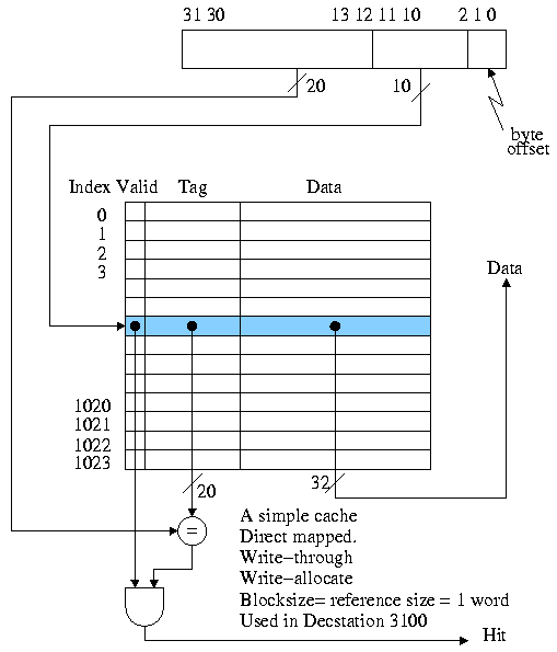
Calculate on the board the total number of bits in this cache.
Homework:
7.1 7.2 7.3
Processing a read for this simple cache.
-
The action required for a hit is obvious, namely return the data
found to the processor.
-
For a miss, the action best action is clear, but not completely
obvious.
- Clearly we must go to central memory to fetch the requested
data since it is not available in the cache.
- The only question is should we place this new data in the
cache replacing the old, or should we maintain the old.
- But it is clear that we want to store the new data instead of
the old.
- Why?
Ans: Temporal Locality
- What do we do with the old data, can we just toss it or do we
need to write it back to central memory.
Ans: It depends! We will see shortly that the action needed on a
read miss, depends on our action for write hits.
Skip the section ``handling cache misses'' as it discusses the
multicycle and pipelined implementations of chapter 6, which we
skipped. For our single cycle processor implementation we just need
to note a few points.
- The instruction and data memory are replaced with caches.
- On cache misses one needs to fetch/store the desired
datum or instruction from/to central memory.
- This is very slow and hence our cycle time must be very
long.
- A major reason why the single cycle implementation is
not used in practice.
Processing a write for our simple cache (direct mapped with block
size = reference size = 1 word).
-
We have 4 possibilities:
-
For a write hit we must choose between
Write through and Write back.
-
Write through: Write the data to memory as well as to the cache.
-
Write back: Don't write to memory now, do it
later when this cache block is evicted.
-
Thus the write hit policy effects our read miss policy as
mentioned just above.
-
For a write miss we must choose between
write-allocate and
write-no-allocate
(also called
store-allocate and
store-no-allocate).
-
Write-allocate:
-
Write the new data into the cache.
-
If the cache is write through, discard the old data
(since it is in memory) and write the new data to memory.
-
If the cache is write back, the old data must now be
written back to memory, but the new data is not
written to memory.
-
Write-no-allocate:
-
Leave the cache alone and just write central memory
with the new data.
-
Not as popular since temporal locality favors
write-allocate.
-
The simplist is write-through, write-allocate.
-
We are still assuming block size = reference size = 1 word and
direct mapped.
-
For any write (hit or miss) do the following:
-
Index the cache using the correct LOBs (i.e., not the very
lowest order bits as these give the byte offset).
-
Write the data and the tag into the cache.
- For a hit, we are overwriting the tag with itself.
- For a miss, we are performing a write allocate and,
since the cache is write-through, memory is guaranteed to
be correct, we can simply overwrite the current entry.
-
Set Valid to true.
-
Send request to main memory.
-
Poor performance
-
For the GCC benchmark 11% of the operations are stores.
-
If we assume an infinite speed central memory (i.e., a
zero miss penalty) or a zero miss rate, the CPI is 1.2 for
some reasonable estimate of instruction speeds.
-
If we assume a 10 cycle store penalty (conservative) since
we have to write main memory (recall we are using a
write-through cache), then the
CPI becomes 1.2 + 10 * 11% = 2.5, which is
half speed.
Improvement: Use a write buffer
- Hold a few (four is common) writes at the processor while they are
being processed at memory.
- As soon as the word is written into the write buffer, the
instruction is considered complete and the next instruction can
begin.
- Hence the write penalty is eliminated as long as the word can be
written into the write buffer.
- Must stall (i.e., incur a write penalty) if the write buffer is
full. This occurs if a bunch of writes occur in a short period.
- If the rate of writes is greater than the rate at which memory can
handle writes, you must stall eventually. The purpose of a
write-buffer (indeed of buffers in general) is to handle short bursts.
- The Decstation 3100 (which employed the simple cache structure
just described) had a 4-word write buffer.
Unified vs split I and D (instruction and data) caches
- Given a fixed total size (in bytes) for caches, is it better to have two
caches, one for instructions and one for data; or is it better to have
a single ``unified'' cache?
-
Unified is better because it automatically performs ``load
balancing''. If the current program needs more data references
than instruction references, the cache will accommodate.
Similarly if more instruction references are needed.
-
Split is better because it can do two references at once (one
instruction reference and one data reference).
-
The winner is ...
split I and D.
-
But unified has the better (i.e. higher) hit ratio.
-
So hit ratio is not the ultimate measure of good cache
performance.
======== START LECTURE #20
========
Improvement: Blocksize > Wordsize
-
The current setup does not take any advantage of spatial locality.
The idea of having a multiword blocksizes is to bring in words near
the referenced word since, by spatial locality, they are likely to
be referenced in the near future.
-
The figure below shows a 64KB direct mapped cache with 4-word
blocks.
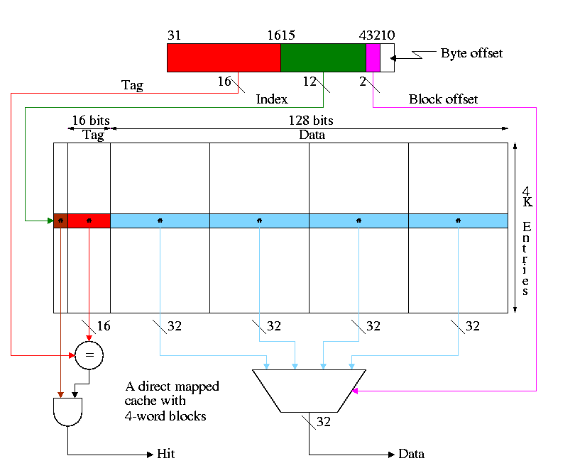
-
What addresses in memory are in the block and where in the cache
do they go?
- The memory block number =
the word address / number of words per block =
the byte address / number of bytes per block
- The cache block number =
the memory block number modulo the number of blocks in the cache
- The block offset =
the word address modulo the number of words per block
- The tag =
the word addres / the number of words in the cache =
the byte address / the number of bytes in the cache
- Show from the diagram how this gives the red portion for the
tag and the green portion for the index or cache block number.
- Consider the cache shown in the diagram above and a reference to
word 17001.
- 17003 / 4 gives 4250 with a remainder of 3 .
- So the memory block number is 4250 and the block offset is 3.
- 4K=4096 and 4250 / 4096 gives 1 with a remainder of 154.
- So the cache block number is 154.
- Putting this together a reference to word 17003 is a reference
to the third word of the cache block with index 154
- The tag is 17003 / (4K * 4) = 1
-
Cachesize = Blocksize * #Entries. For the diagram above this is 64KB.
-
Calculate the total number of bits in this cache and in one
with one word blocks but still 64KB of data.
-
If the references are strictly sequential the pictured cache has 75% hits;
the simplier cache with one word blocks has no
hits.
-
How do we process read/write hits/misses?
-
Read hit: As before, return the data found to the processor.
-
Read miss: As before, due to locality we discard (or write
back) the old line and fetch the new line.
-
Write hit: As before, write the word in the cache (and perhaps
write memory as well).
-
Write miss: A new consideration arises. As before we might or
might not decide to replace the current line with the
referenced line. The new consideration is that if we decide
to replace the line (i.e., if we are implementing
store-allocate), we must remember that we only have a new
word and the unit of cache transfer is a
multiword line.
-
The simplest idea is to fetch the entire old line and
overwrite the new word. This is called
write-fetch and is something you wouldn't
even consider with blocksize = reference size = 1 word.
-
Why fetch the whole line including the word you are going
to overwrite?
Ans. The memory subsystem probably can't fetch just words
1,2, and 4 of the line.
-
Why might we want store-allocate and
write-no-fetch?
-
Ans: Because a common case is storing consecutive words:
With store-no-allocate all are misses and with
write-fetch, each store fetches the line to
overwrite another part of it.
-
To implement store-allocate-no-write-fetch (SANF), we need
to keep a valid bit per word.
Homework:
7.7 7.8 7.9
Why not make blocksize enormous? For example, why not have the cache
be one huge block.
-
NOT all access are sequential.
-
With too few blocks misses go up again.
Memory support for wider blocks
-
Should memory be wide?
-
Should the bus from the cache to the processor be wide?
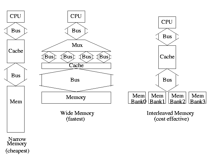
-
Assume
-
1 clock required to send the address. Only one address is
needed per access for all designs.
-
15 clocks are required for each memory access (independent of
width).
-
1 Clock/busload required to transfer data.
-
How long does it take satisfy a read miss for the cache above and
each of the three memory/bus systems.
-
Narrow design (a) takes 65 clocks: 1 address transfer, 4 memory
reads, 4 data transfers (do it on the board).
-
Wide design (b) takes 17.
-
Interleaved design (c) takes 20.
-
Interleaving works great because in this case we are
guaranteed to have sequential accesses.
-
Imagine a design between (a) and (b) with a 2-word wide datapath.
It takes 33 cycles and is more expensive to build than (c).
Homework: 7.11
7.3: Measuring and Improving Cache Performance
Performance example to do on the board (a dandy exam question).
-
Assume
-
5% I-cache miss.
-
10% D-cache miss.
-
1/3 of the instructions access data.
-
CPI = 4 if miss penalty is 0 (A 0 miss penalty is not
realistic of course).
-
What is CPI with miss penalty 12 (do it)?
-
What is CPI if we upgrade to a double speed cpu+cache, but keep a
single speed memory (i.e., a 24 clock miss penalty)?
Do it on the board.
-
How much faster is the ``double speed'' machine? It would be double
speed if the miss penalty were 0 or if there was a 0% miss rate.
Homework:
7.15, 7.16
======== START LECTURE #21
========
A lower base (i.e. miss-free) CPI makes stalls appear more expensive
since waiting a fixed amount of time for the memory
corresponds to losing more instructions if the CPI is lower.
A faster CPU (i.e., a faster clock) makes stalls appear more expensive
since waiting a fixed amount of time for the memory corresponds to
more cycles if the clock is faster (and hence more instructions since
the base CPI is the same).
Another performance example.
- Assume
- I-cache miss rate 3%.
- D-cache miss rate 5%.
- 40% of instructions reference data.
- miss penalty of 50 cycles.
- Base CPI is 2.
- What is the CPI including the misses?
- How much slower is the machine when misses are taken into account?
- Redo the above if the I-miss penalty is reduced to 10 (D-miss
still 50)
- With I-miss penalty back to 50, what is performance if CPU (and the
caches) are 100 times faster
Remark: Larger caches have longer hit times.
Improvement: Associative Caches
Consider the following sad story. Jane has a cache that holds 1000
blocks and has a program that only references 4 (memory) blocks,
namely 23, 1023, 123023, and 7023. In fact the references occur in
order: 23, 1023, 123023, 7023, 23, 1023, 123023, 7023, 23, 1023,
123023, 7023, 23, 1023, 123023, 7023, etc. Referencing only 4 blocks
and having room for 1000 in her cache, Jane expected an extremely high
hit rate for her program. In fact, the hit rate was zero. She was so
sad, she gave up her job as webmistriss, went to medical school, and
is now a brain surgeon at the mayo clinic in rochester MN.
So far We have studied only direct mapped caches,
i.e. those for which the location in the cache is determined by
the address. Since there is only one possible location in the
cache for any block, to check for a hit we compare one
tag with the HOBs of the addr.
The other extreme is fully associative.
-
A memory block can be placed in any cache block.
-
Since any memory block can be in any cache block, the cache index
where the memory block is stored tells us nothing about which
cache block is stored there. Hence the tag must be the entire
address. Moreover, we don't know which cache block to check so we
must check all cache blocks to see if we have a hit.
-
The larger tag is a problem.
-
The search is a disaster.
- It could be done sequentially (one cache block at a time),
but this is much too slow.
- We could have a comparator with each tag and mux
all the blocks to select the one that matches.
- This is too big due to both the many comparators and
the humongous mux.
- However, it is exactly what is done when implementing
translation lookaside buffers (TLBs), which are used with
demand paging.
- Are the TLB designers magicians?
Ans: No. TLBs are small.
-
An alternative is to have a table with one entry per
MEMORY block giving the cache block number. This is too
big and too slow for caches but is used for virtual memory
(demand paging).
Most common for caches is an intermediate configuration called
set associative or n-way associative (e.g., 4-way
associative).
- n is typically 2, 4, or 8.
- If the cache has B blocks, we group them into B/n
sets each of size n. Memory block number K is
then stored in set K mod (B/n).
- Figure 7.15 has a bug. It indicates that the tag for memory
block 12 is 12 for all associativitiese. The figure below
corrects this.
- In the picture we are trying to store memory block 12 in each
of three caches.
- The light blue represents cache blocks in which the memory
block might have been stored.
- The dark blue is the cache block in which the memory block
is stored.
- The arrows show the blocks (i.e., tags) that must be
searched to look for memory block 12. Naturally the arrows
point to the blue blocks.
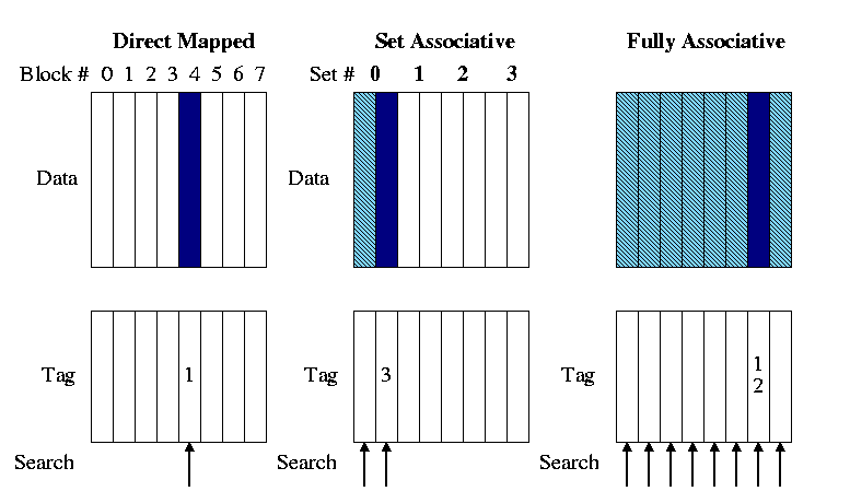
-
The picture shows 2-way set set associative. Do on the board
4-way set associative.
-
Determining the Set# and Tag.
- The Set# = (memory) block# mod #sets.
- The Tag = (memory) block# / #sets.
-
Ask in class.
- What is 8-way set associative in a cache with 8 blocks (i.e.,
the cache in the picture)?
- What is 1-way set associative?
-
Why is set associativity good? For example, why is 2-way set
associativity better than direct mapped?
-
Consider referencing two modest arrays (<< cache size) that
start at location 1MB and 2MB.
-
Both will contend for the same cache locations in a direct
mapped cache but will fit together in an n-way associative
cache with n>=2.
======== START LECTURE #22
========
-
How do we find a memory block in an associative cache (with
block size 1 word)?
- Divide the memory block number by the number of sets to get
the index into the cache.
- Mod the memory block number by the number of sets to get the tag.
- Check all the tags in the set against the tag of the
memory block.
- If any tag matches, a hit has occurred and the
corresponding data entry contains the memory block.
- If no tag matches, a miss has occurred.
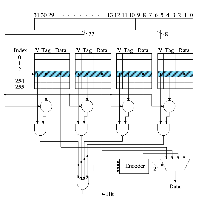
-
Why is set associativity bad?
Ans: It is a little slower due to the mux and AND gate.
-
Which block (in the set) should be replaced?
-
Random is sometimes used.
- But it is not used for paging!
- The number of blocks in a set is small, so the likely
difference in quality between the best and the worst is less.
- For caches, speed is crucial so have no time for
calculations, even for misses.
-
LRU is better, but not easy to do quickly.
-
If the cache is 2-way set associative, each set is of size
two and it is easy to find the lru block quickly.
How?
Ans: For each set keep a bit indicating which block in the set
was just referenced and the lru block is the other one.
-
If the cache is 4-way set associative, each set is of size
4. Consider these 4 blocks as two groups of 2. Use the
trick above to find the group most recently used and pick
the other group. Also use the trick within each group and
chose the block in the group not used last.
-
Sound great. We can do lru fast for any power of two using
a binary tree.
-
Wrong! The above is
not LRU it is just an approximation. Show this on the board.
-
Sizes
- How big is the cache? This means, what is the capacity?
Ans: 256 * 4 * 4B = 4KB.
- How many bits are in the cache?
- Answer
- The 32 address bits contain 8 bits of index and 2 bits
giving the byte offset.
- So the tag is 22 bits (more examples
just below).
- Each block contains 1 valid bit, 22 tag bits and 32 data
bits, for a total of 55 bits.
- There are 1K blocks.
- So the total size is 55Kb (kilobits).
- What fraction of the bits are user data?
Ans: 4KB / 53Kb = 32Kb / 53Kb = 32/53.
Tag size and division of the address bits
We continue to assume a byte addressed machines with all references
to a 4-byte word (lw and sw).
The 2 LOBs are not used (they specify the byte within the word but
all our references are for a complete word). We show these two bits in
dark blue.
We continue to assume 32
bit addresses so there are 2**30 words in the address space.
Let's review various possible cache organizations and determine for
each how large is the tag and how the various address bits are used.
We will always use a 16KB cache. That is the size of the
data portion of the cache is 16KB = 4 kilowords =
2**12 words.
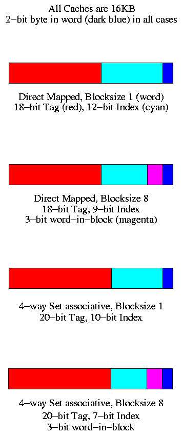
- Direct mapped, blocksize 1 (word).
- Since the blocksize is one word, there are 2**30 memory blocks
and all the address bits (except the 2 LOBs that specify the byte
within the word) are used for the memory block number.
Specifically 30 bits are so used.
- The cache has 2**12 words, which is 2**12 blocks.
- So the low order 12 bits of the memory block number give the
index in the cache (the cache block number), shown in cyan.
- The remaining 18 (30-12) bits are the tag, shown in red.
- Direct mapped, blocksize 8
- Three bits of the address give the word within the 8-word
block. These are drawn in magenta.
- The remaining 27 HOBs of the
memory address give the memory block number.
- The cache has 2**12 words, which is 2**9 blocks.
- So the low order 9 bits of the memory block number gives the
index in the cache.
- The remaining 18 bits are the tag
- 4-way set associative, blocksize 1
- Blocksize is 1 so there are 2**30 memory blocks and 30 bits
are used for the memory block number.
- The cache has 2**12 blocks, which is 2**10 sets (each set has
4=2**2 blocks).
- So the low order 10 bits of the memory block number gives
the index in the cache.
- The remaining 20 bits are the tag.
- As the associativity grows, the tag gets bigger. Why?
Ans: Growing associativity reduces the number of sets into which a
block can be placed. This increases the number of memory blocks
eligible tobe placed in a given set. Hence more bits are needed
to see if the desired block is there.
- 4-way set associative, blocksize 8
- Three bits of the address give the word within the block.
- The remaining 27 HOBs of the
memory address give the memory block number.
- The cache has 2**12 words = 2**9 blocks = 2**7 sets.
- So the low order 7 bits of the memory block number gives
the index in the cache.
Homework: 7.39, 7.40
Improvement: Multilevel caches
Modern high end PCs and workstations all have at least two levels
of caches: A very fast, and hence not very big, first level (L1) cache
together with a larger but slower L2 cache.
When a miss occurs in L1, L2 is examined, and only if a miss occurs
there is main memory referenced.
So the average miss penalty for an L1 miss is
(L2 hit rate)*(L2 time) + (L2 miss rate)*(L2 time + memory time)
We are assuming L2 time is the same for an L2 hit or L2 miss. We are
also assuming that the access doesn't begin to go to memory until the
L2 miss has occurred.
Do an example
- Assume
- L1 I-cache miss rate 4%
- L2 D-cache miss rate 5%
- 40% of instructions reference data
- L2 miss rate 6%
- L2 time of 15ns
- Memory access time 100ns
- Base CPI of 2
- Clock rate 400MHz
- How many instructions per second does this machine execute
- How many instructions per second would this machine execute if
the L2 cache were eliminated.
- How many instructions per second would this machine execute if
both caches were eliminated.
- How many instructions per second would this machine execute if the
L2 cache had a 0% miss rate (L1 as originally specified).
- How many instructions per second would this machine execute if
both L1 caches had a 0% miss rate
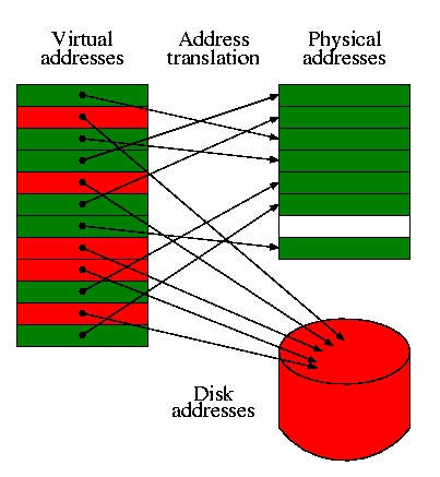
7.4: Virtual Memory
I realize this material was covered in operating systems class
(V22.0202). I am just reviewing it here. The goal is to show the
similarity to caching, which we just studied. Indeed, (the demand
part of) demand paging is caching: In demand paging the
memory serves as a cache for the disk, just as in caching the cache
serves as a cache for the memory.
The names used are different and there are other differences as well.
| Cache concept | Demand paging analogue |
|---|
| Memory block | Page |
| Cache block | Page Frame (frame) |
| Blocksize | Pagesize |
| Tag | None (table lookup) |
| Word in block | Page offset |
| Valid bit | Valid bit |
| Miss | Page fault |
| Hit | Not a page fault |
| Miss rate | Page fault rate |
| Hit rate | 1 - Page fault rate |
| Cache concept | Demand paging analogue |
|---|
| Placement question | Placement question |
| Replacement question | Replacement question |
| Associativity | None (fully associative) |
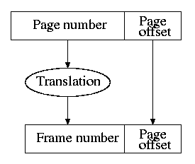
- For both caching and demand paging, the placement
question is trivial since the items are fixed size (no first-fit,
best-fit, buddy, etc).
- The replacement question is not trivial. (H&P
list this under the placement question, which I believe is in error).
Approximations to LRU are popular for both caching and demand
paging.
- The cost of a page fault vastly exceeds the cost of a cache miss
so it is worth while in paging to slow down hit processing to lower
the miss rate. Hence demand paging is fully associative and uses a
table to locate the frame in which the page is located.
- The figures to the right are for demand paging. But they can be
interpreted for caching as well.
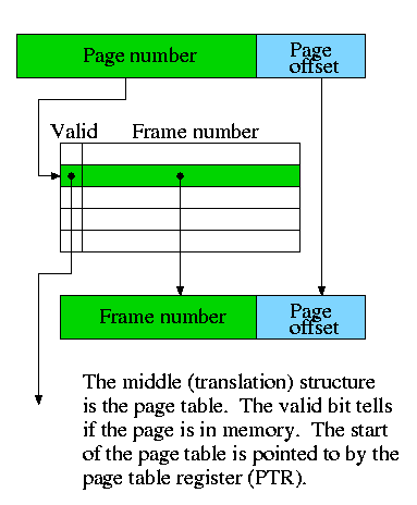
- The (virtual) page number is the memory block number
- The Page offset is the word-in-block
- The frame (physical page) number is the cache block number
(which is the index into the cache).
- Since demand paging uses full associativity, the tag is the
entire memory block number. Instead of checking every cache block
to see if the tags match, a (page) table is used.
Homework: 7.32
Write through vs. write back
Question: On a write hit should we write the new value through to
(memory/disk) or just keep it in the (cache/memory) and write it back
to (memory/disk) when the (cache-line/page) is replaced?
- Write through is simpler since write back requires two operations
at a single event.
- But write-back has fewer writes to (memory/disk) since multiple
writes to the (cache-line/page) may occur before the (cache-line/page)
is evicted.
- For caching the cost of writing through to memory is probably less
than 100 cycles so with a write buffer the cost of write through is
bearable and it does simplify the situation.
- For paging the cost of writing through to disk is on the order of
1,000,000 cycles. Since write-back has fewer writes to disk, it is used.
======== START LECTURE #23
========
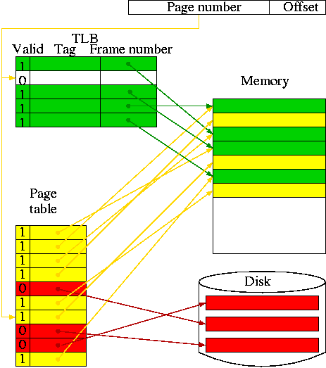
Translation Lookaside Buffer (TLB)
A TLB is a cache of the page table
- Needed because otherwise every memory reference in the program
would require two memory references, one to read the page table and
one to read the requested memory word.
- Typical TLB parameter values
- Size: hundreds of entries.
- Block size: 1 entry.
- Hit time: 1 cycle.
- Miss time: tens of cycles.
- Miss rate: Low (<= 2%).
- In the diagram on the right:
- The green path is the fastest (TLB hit).
- The red is the slowest (page fault).
- The yellow is in the middle (TLB miss, no page fault).
- Really the page table doesn't point to the disk block for an
invalid entry, but the effect is the same.
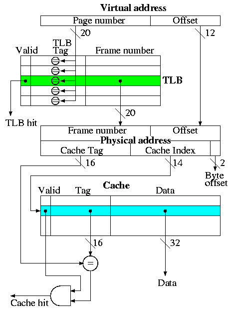
Putting it together: TLB + Cache
This is the decstation 3100
- Virtual address = 32 bits
- Physical address = 32 bits
- Fully associative TLB (naturally)
- Direct mapped cache
- Cache blocksize = one word
- Pagesize = 4KB = 2^12 bytes
- Cache size = 16K entries = 64KB
Actions taken
- The page number is searched in the fully associative TLB
- If a TLB hit occurs, the frame number from the TLB together with
the page offset gives the physical address. A TLB miss causes an
exception to reload the TLB from the page table, which the figure does
not show.
- The physical address is broken into a cache tag and cache index
(plus a two bit byte offset that is not used for word references).
- If the reference is a write, just do it without checking for a
cache hit (this is possible because the cache is so simple as we
discussed previously).
- For a read, if the tag located in the cache entry specified by the
index matches the tag in the physical address, the referenced word has
been found in the cache; i.e., we had a read hit.
- For a read miss, the cache entry specified by the index is fetched
from memory and the data returned to satisfy the request.
Hit/Miss possibilities
| TLB | Page | Cache | Remarks |
|---|
| hit | hit | hit |
Possible, but page table not checked on TLB hit, data from cache |
| hit | hit | miss |
Possible, but page table not checked, cache entry loaded from memory |
| hit | miss | hit |
Impossible, TLB references in-memory pages |
| hit | miss | miss |
Impossible, TLB references in-memory pages |
| miss | hit | hit |
Possible, TLB entry loaded from page table, data from cache |
| miss | hit | miss |
Possible, TLB entry loaded from page table, cache entry loaded from memory |
| miss | miss | hit |
Impossible, cache is a subset of memory |
| miss | miss | miss |
Possible, page fault brings in page, TLB entry loaded, cache loaded |
Homework: 7.31, 7.33
7.5: A Common Framework for Memory Hierarchies
Question 1: Where can/should the block be placed?
This question has three parts.
- In what slot are we able to place the block.
- For a direct mapped cache, there is only one choice.
- For an n-way associative cache, there are n choices.
- For a fully associative cache, any slot is permitted.
- The n-way case includes both the direct mapped and fully
associative cases.
- For a TLB any slot is permitted. That is, a TLB is a fully
associative cache of the page table.
- For paging any slot (i.e., frame) is permitted. That is,
paging uses a fully associative mapping (via a page table).
- For segmentation, any large enough slot (i.e., region) can be
used.
- If several possible slots are available, which one should
be used?
- I call this question the placement question.
- For caches, TLBs and paging, which use fixed size
slots, the question is trivial; any available slot is just fine.
- For segmentation, the question is interesting and there are
several algorithms, e.g., first fit, best fit, buddy, etc.
- If no possible slots are available, which victim should be chosen?
- For direct mapped caches, the question is trivial. Since the
block can only go in one slot, if you need to place the block and
the only possible slot is not available, it must be the victim.
- For all the other cases, n-way associative caches (n>1), TLBs
paging, and segmentation, the question is interesting and there
are several algorithms, e.g., LRU, Random, Belady min, FIFO, etc.
- See question 3, below.
Question 2: How is a block found?
| Associativity | Location method | Comparisons Required |
|---|
| Direct mapped | Index | 1 |
| Set Associative | Index the set, search among elements
| Degree of associativity |
| Full | Search all cache entries
| Number of cache blocks |
| Separate lookup table | 0 |
Typical sizes and costs
| Feature |
Typical values
for caches |
Typical values
for demand paging |
Typical values
for TLBs |
| Size |
8KB-8MB |
16MB-2GB |
256B-32KB |
| Block size |
16B-256B |
4KB-64KB |
4B-32B |
| Miss penalty in clocks |
10-100 |
1M-10M |
10-100 |
| Miss rate |
.1%-10% |
.000001-.0001% |
.01%-2% |
|
The difference in sizes and costs for demand paging vs. caching,
leads to different algorithms for finding the block.
Demand paging always uses the bottom row with a separate table (page
table) but caching never uses such a table.
- With page faults so expensive, misses must be reduced as much as
possible. Hence full associativity is used.
- With such a large associativity (fully associative with many
slots), hardware would be prohibitively expensive and software
searching too slow. Hence a page table is used with a TLB acting as a
cache.
- The large block size (called the page size) means that the extra table
is a small fraction of the space.
Question 3: Which block should be replaced?
This is called the replacement question and is much
studied in demand paging (remember back to 202).
- For demand paging, with miss costs so high and associativity so
large, the replacement policy is very important and some approximation
to LRU is used.
- For caching, even the miss time must be small so simple schemes
are used. For 2-way associativity, LRU is trivial. For higher
associativity (but associativity is never very high) crude
approximations to LRU may be used and sometimes even random
replacement is used.
======== START LECTURE #24
========
Question 4: What happens on a write?
- Write-through
- Data written to both the cache and main memory (in general to
both levels of the hierarchy).
- Sometimes used for caching, never used for demand paging.
- Advantages
- Misses are simpler and cheaper (no copy back).
- Easier to implement, especially for block size 1, which we
did in class.
- For blocksize > 1, a write miss is more complicated since
the rest of the block now is invalid. Fetch the rest of the
block from memory (or mark those parts invalid by extra valid
bits--not covered in this course).
Homework: 7.41
- Write-back
- Data only written to the cache. The memory has stale data,
but becomes up to date when the cache block is subsequently
replaced in the cache.
- Only real choice for demand paging since writing to the lower
level of the memory hierarch (in this case disk) is so slow.
- Advantages
- Words can be written at cache speed not memory speed
- When blocksize > 1, writes to multiple words in the cache
block are only written once to memory (when the block is
replaced).
- Multiple writes to the same word in a short period are
written to memory only once.
- When blocksize > 1, the replacement can utilize a high
bandwidth transfer. That is, writing one 64-byte block is
faster than 16 writes of 4-bytes each.
Write miss policy (advanced)
- For demand paging, the case is pretty clear. Every
implementation I know of allocates frame for the page miss and
fetches the page from disk. That is it does both an
allocate and a fetch.
- For caching this is not always the case. Since there are two
optional actions there are four possibilities.
- Don't allocate and don't fetch: This is sometimes called
write around. It is done when the data is not expected to be
read before it will be evicted. For example, if you are
writing a matrix whose size is much larger than the cache.
- Don't allocate but do fetch: Impossible, where would you
put the fetched block?
- Do allocate, but don't fetch: Sometimes called
no-fetch-on-write. Also called SANF
(store-allocate-no-fetch). Requires multiple valid bits per
block since the just-written word is valid but the others are
not (since we updated the tag to correspond to the
just-written word).
- Do allocate and do fetch: The normal case we have been
using.
Chapter 8: Interfacing Processors and Peripherals.
With processor speed increasing 50% / year, I/O must improved or
essentially all jobs will be I/O bound.
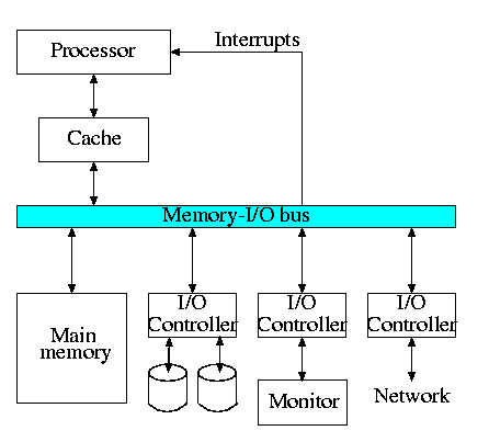
The diagram on the right is quite oversimplified for modern PCs; a
more detailed version is below.
8.2: I/O Devices
Devices are quite varied and their data rates vary enormously.
- Some devices like keyboards and mice have tiny data rates.
- Printers, etc have moderate data rates.
- Disks and fast networks have high data rates.
- A good graphics card and monitor has a huge data rate.
Show a real disk opened up and illustrate the components
- Platter
- Surface
- Head
- Track
- Sector
- Cylinder
- Seek time
- Rotational latency
- Transfer time
8.4: Buses
A bus is a shared communication link, using one set of wires to
connect many subsystems.
- Sounds simple (once you have tri-state drivers) ...
- ... but it's not.
- Very serious electrical considerations (e.g. signals reflecting
from the end of the bus. We have ignored (and will continue to
ignore) all electrical issues.
- Getting high speed buses is state-of-the-art engineering.
- Tri-state drivers (advanced):
- A output device that can either
- Drive the line to 1.
- Drive the line to 0.
- Not drive the line at all (be in a high impedance state).
- It is possible have many of these devices devices connected to
the same wire providing you are careful to be sure that all
but one are in the high-impedance mode.
- This is why a single bus can have many output devices attached
(but only one actually performing output at a given time).
- Buses support bidirectional transfer, sometimes using separate
wires for each direction, sometimes not.
- Normally the memory bus is kept separate from the I/O bus. It is
a fast synchronous bus (see next section) and I/O
devices can't keep up.
- Indeed the memory bus is normally custom designed (i.e., companies
design their own).
- The graphics bus is also kept separate in modern designs for
bandwidth reasons, but is an industry standard (the so called AGP
bus).
- Many I/O buses are industry standards (ISA, EISA, SCSI, PCI) and
support open architectures, where components can
be purchased from a variety of vendors.
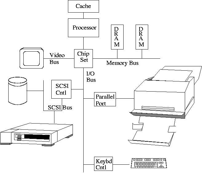
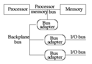
- The figure above is similar to H&P's figure 8.9(c), which is
shown on the right. The primary difference is that they have the
processor directly connected to the memory with a processor memory
bus.
- The processor memory bus has the highest bandwidth, the backplane
bus less and the I/O buses the least. Clearly the (sustained)
bandwidth of each I/O bus is limited by the backplane bus.
Why?
Because all the data passing on an I/O bus must also pass on the
backplane bus. Similarly the backplane bus clearly has at least
the bandwidth of an I/O bus.
- Bus adaptors are used as interfaces between buses. They perform
speed matching and may also perform buffering, data width
matching, and converting between synchronous and
asynchronous buses (see next section).
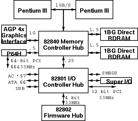
- For a realistic example, on the right is a diagram adapted from
the 25 October 1999 issue of Microprocessor Reports on a
then new Intel chip set, the so called 840.
- Bus adaptors have a variety of names, e.g. host adapters, hubs,
bridges.
- Bus lines (i.e., wires) include those for data (data lines),
function codes, device addresses. Data and address are considered
data and the function codes are considered control (remember our
datapath for MIPS).
- Address and data may be multiplexed on the same lines (i.e., first
send one then the other) or may be given separate lines. One is
cheaper (good) and the other has higher performance (also
good). Which is which?
Ans: the multiplexed version is cheaper.
Synchronous vs. Asynchronous Buses
A synchronous bus is clocked.
- One of the lines in the bus is a clock that serves as the clock
for all the devices on the bus.
- All the bus actions are done on fixed clock cycles. For example,
4 cycles after receiving a request, the memory delivers the first
word.
- This can be handled by a simple finite state machine (FSM).
Basically, once the request is seen everything works one clock at
a time. There are no decisions like the ones we will see for an
asynchronous bus.
- Because the protocol is so simple, it requires few gates and is
very fast. So far so good.
- Two problems with synchronous buses.
- All the devices must run at the same speed.
- The bus must be short due to clock skew.
- Processor to memory buses are now normally synchronous.
- The number of devices on the bus are small.
- The bus is short.
- The devices (i.e. processor and memory) are prepared to run at
the same speed.
- High speed is crucial.
An asynchronous bus is not clocked.
- Since the bus is not clocked devices of varying speeds can be on the
same bus.
- There is no problem with clock skew (since there is no clock).
- But the bus must now contain control lines to coordinate
transmission.
- Common is a handshaking protocol.
- We now describe a protocol in words and with FSM for a device to obtain
data from memory.
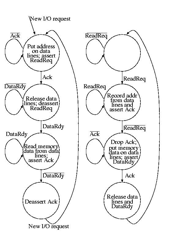
- The device makes a request (asserts ReadReq and puts the
desired address on the data lines).
- Memory, which has been waiting, sees ReadReq, records the
address and asserts Ack.
- The device waits for the Ack; once seen, it drops the
data lines and deasserts ReadReq.
- The memory waits for the request line to drop. Then it can drop
Ack (which it knows the device has now seen). The memory now at its
leasure puts the data on the data lines (which it knows the device is
not driving) and then asserts DataRdy. (DataRdy has been deasserted
until now).
- The device has been waiting for DataRdy. It detects DataRdy and
records the data. It then asserts Ack indicating that the data has
been read.
- The memory sees Ack and then deasserts DataRdy and releases the
data lines.
- The device seeing DataRdy low deasserts Ack ending the show. Note
that both sides are prepared for another performance.
Improving Bus Performance
These improvements mostly come at the cost of increased expense and/or
complexity.
- A multiplicity of buses as the diagrams above.
- Synchronous instead of asynchronous protocols. >Synchronous is
actually simplier, but it essentially implies a
multiplicity of buses, since not all devices can operate at the
same speed.
>br>
- Wider data path: Use more wires, send more data at one time.
- Separate address and data lines: Same as above.
- Block transfers: Permit a single transaction to transfer more than
one busload of data. Saves the time to release and acquire the
bus, but the protocol is more complex.
======== START LECTURE #25
========
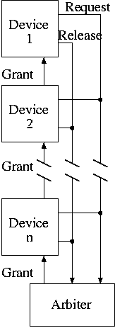
Obtaining bus access
- The simplest scheme is to permit only one bus
master.
- That is, on each bus only one device is permited to
initiate a bus transaction.
- The other devices are slaves that only
respond to requests.
- With a single master, there is no issue of arbitrating
among multiple requests.
- One can have multiple masters with daisy
chaining of the grant line.
- Any device can assert the request line, indicating that it
wishes to use the bus.
- This is not trivial: uses ``open collector drivers''.
- If no output drives the line, it will be ``pulled up'' to
5v, i.e., a logical true.
- If one or more outputs drive the line to 0v it will go to
0v (a logical false).
- So if a device wishes to make a request it drives the line
to 0v; if it does not wish to make a request it does nothing.
- This is (another example of) active low logic. The
request line is asserted by driving it low.
- When the arbiter sees the request line asserted (and the
previous grantee has issued a release), the arbiter raises the
grant line.
- The grant signal is passed from one device to another if the
first device is not requesting the bus. Hence
devices near the arbiter have priority and can starve the ones
further away.
- The device whose request is granted asserts the release line
when done.
- Simple, but not fair and not of high performance.
- Centralized parallel arbiter: Separate request lines from each
device and separate grant lines. The arbiter decides which device
should be granted the bus.
- Distributed arbitration by self-selection: Requesting
processes identify themselves on the bus and decide individually
(and consistently) which one gets the grant.
- Distributed arbitration by collision detection: Each device
transmits whenever it wants, but detects collisions and retries.
Ethernet uses this scheme (but modern switched ethernets do not).
| Option | High performance | Low cost |
|---|
| bus width | separate addr and data lines |
multiplex addr and data lines |
| data width | wide | narrow |
| transfer size | multiple bus loads | single bus loads |
| bus masters | multiple | single |
| clocking | synchronous | asynchronous |
Do on the board the example on pages 665-666
- Memory and bus support two widths of data transfer: 4 words and 16
words
- 64-bit synchronous bus; 200MHz; 1 clock for addr; 1 for data.
- Two clocks of ``rest'' between bus accesses
- Memory access times: 4 words in 200ns; additional 4 word blocks in
20ns per block.
- Can overlap transferring data with reading next data.
- Find
- Sustained bandwidth and latency for reading 256 words using
both size transfers
- How many bus transactions per sec for each (addr+data)
- Four word blocks
- 1 clock to send addr
- 40 clocks read mem
- 2 clocks to send data
- 2 idle clocks
- 45 total clocks
- 256/4=64 transactions needed so latency is 64*45*5ns=14.4us
- 64 trans per 14.4us = 64/14.4 trans per 1us = 4.44M trans per
sec
- Bandwidth = 1024 bytes per 14.4us = 1024/14.4 B/us = 71.11MB/sec
- Sixteen word blocks
- 1 clock for addr
- 40 clocks for reading first 4 words
- 2 clocks to send
- 2 clocks idle
- 4 clocks to read next 4 words. But this is free! Why?
Because it is done during the send and idle of previous block.
- So we only pay for the long initial read
- Total = 1 + 40 + 4*(2+2) = 57 clocks.
- 16 transactions need; latency = 57*16*5ns=4.56ms, which is
much better than with 4 word blocks.
- 16 transactions per 4.56us = 3.51M transactions/sec
- Bandwidth = 1024B per 4.56ms = 224.56MB/sec
======== START LECTURE #26
========
Notes:
I received the official final exam notice from robin.
V22.0436.001   Gottlieb    Weds. 12/20      WWH 109
                           2:00-3:50pm
Last year's final exam is on the course home page.
End of Notes
8.5: Interfacing I/O Devices
Giving commands to I/O Devices
This is really an OS issue. Must write/read to/from device
registers, i.e. must communicate commands to the controller. Note
that a controller normally contains a microprocessor, but when we say
the processor, we mean the central processor not the one on the
controller.
- The controler has a few registers that can be read and/or written
by the processor, similar to how the processor reads and writes
memory. These registers are also read and written by the controller.
- Nearly every controler contains
- A data register, which is readable (by the processor) for an
input device (e.g., a simple keyboard), writable for an output
device (e.g., a simple printer), and both readable and writable
for input/output devices (e.g., disks).
- A control register for giving commands to the device.
- A readable status register for reporting errors and announcing
when the device is ready for the next action (e.g., for a keyboard
telling when the data register is valid, and for a printer telling
when the character to be printed has be successfully retrieved
from the data register). Remember the communication protocol we
studied where ack was used.
- Many controllers have more registers
Communicating with the Processor
Should we check periodically or be told when there is something to
do? Better yet can we get someone else to do it since we are not
needed for the job?
- We get mail at home once a day.
- At some business offices mail arrives a few times per day.
- No problem checking once an hour for mail.
- If email wasn't buffered, you would have to check several times
per minute (second?, milisecond?).
- Checking email this often is too much of a burden and most of the
time when you check you find there is none so the check was wasted.
Polling
Processor continually checks the device status to see if action is
required.
- Like the mail example above.
- For a general purpose OS, one needs a timer to tell the processor
it is time to check (OS issue).
- For an embedded system (microwave) make the checking part of the
main control loop, which is guaranteed to be executed at a minimum
frequency (application software issue).
- For a keyboard or mouse, which have very low data rates, the
system can afford to have the main CPU check.
We do an example just below.
- It is a little better for slave-like output devices such as a
simple printer.
Then the processor only has to poll after a request
has been made until the request has been satisfied.
Do on the board the example on pages 676-677
- Cost of a poll is 400 clocks.
- CPU is 500MHz.
- How much of the CPU is needed to poll
- A mouse that requires 30 polls per sec?
- A floppy that sends 2 bytes at a time and achieves 50KB/sec?
- A hard disk that sends 16 bytes at a time and achieves 4MB/sec?
- For the mouse, we use 12,000 clock cycles each second sec for
polling. The CPU runs at 500*10^6 cycles/sec. So polling the mouse
requires 12/500*10^-3 = 2.4*10^-5 of the CPU. A very small
penalty.
- The floppy delivers 25,000 (two byte) data packets per second so
we must poll at that rate not to miss one. CPU cycles needed each
second is (400)(25,000)=10^7. This represents 10^7 / 500*10^6 = 2% of
the CPU
- To keep up with the disk requires 250K polls/sec or 10^8 clock
cycles or 20% of the CPU.
- The system need not poll the floppy and disk until the
CPU had issues a request. But then it must keep polling until the
request is satisfied.
Interrupt driven I/O
Processor is told by the device when to look. The processor is
interrupted by the device.
- Dedicated lines (i.e. wires) on the bus are assigned for
interrupts.
- When a device wants to send an interrupt it asserts the
corresponding line.
- The processor checks for interrupts after each instruction. This
requires ``zero time'' as it is done in parallel with the
instruction execution.
- If an interrupt is pending (i.e., if a line is asserted) the
processor (this is mostly an OS issue, covered in 202).
- Saves the PC and perhaps some registers.
- Switches to kernel (i.e., privileged) mode.
- Jumps to a location specified in the hardware (the
interrupt handler.
At this point the OS takes over.
- What if we have several different devices and want to do different
things depending on what caused the interrupt?
- Use vectored interrupts.
- Instead of jumping to a single fixed location, the system
defines a set of locations.
- The system might have several interrupt lines. If line 1 is
asserted, jump to location 100, if line 2 is aserted jump to
location 200, etc.
- Alternatively, the system could have just one line
and have the device send the address to jump to.
- There are other issues with interrupts that are taught
in OS. For example, what happens if an interrupt occurs while an
interrupt is being processed. For another example, what if one
interrupt is more important than another. These are OS issues and are
not covered in this course.
- The time for processing an interrupt is typically longer than the
type for a poll. But interrupts are not generated when the
device is idle, a big advantage.
Do on the board the example on pages 681-682.
- Same hard disk and processor as above.
- Cost of servicing an interrrupt is 500 cycles.
- The disk is active only 5% of the time.
- What percent of the processor would be used to service the
interrupts?
- Cycles/sec needed for processing interrupts while the disk is
active is 125 million.
- This represents 25% of the processor cycles available.
- But the true cost is only 1.25%, since the disk is active only 5%
of the time.
- Note that the disk is not active (i.e., actively generating
interrupts) right after the request is made. During the seek and
rotational latency, interrupts are not generated. Only during the
transfer are interrupts generated.
======== START LECTURE #27
========
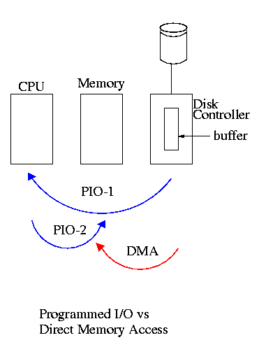
Direct Memory Access (DMA)
The processor initiates the I/O operation then ``something else''
takes care of it and notifies the processor when it is done (or if an
error occurs).
- Have a DMA engine (a small processor) on the controller.
- The processor initiates the DMA by writing the command into data
registers on the controller (e.g., read sector 5, head 4, cylinder
123 into memory location 34500)
- For commands that are longer than the size of the data register(s), a
protocol must be used to transmit the information.
- (I/O done by the processor as in the previous methods is called
programmed I/O, PIO).
- The controller collects data from the device and then sends it on
the bus to the memory without bothering the CPU.
- So we have a multimaster bus and need some sort of
arbitration.
- Normally the I/O devices are given higher priority than the CPU.
- Freeing the CPU from this task is good but isn't as wonderful
as it seems since the memory is busy (but cache hits can be
processed).
- A big gain is that only one bus transaction is needed per bus
load. With PIO, two transactions are needed: controller to
processor and then processor to memory.
- This was for an input operation (the controller writes to
memory). A similar situation occurs for output where the controller
reads from the memory). Once again one bus transaction per bus
load.
- When the controller detects that the I/O is complete or if an
error occurs, it sets the status register accordingly and sends an
interrupt to the processor to notify the latter that the I/O is complete.
More Sophisticated Controllers
- Sometimes called ``intelligent'' device controlers, but I
prefer not to use anthropomorphic terminology.
- Some devices, for example a modem on a serial line, deliver data
without being requested to. So a controller may need to be prepared
for unrequested data.
- Some devices, for example an ethernet, have a complicated
protocol so it is desirable for the controller to process some of that
protocol. In particular, the collision detection and retry with
exponential backoff characteristic of (non-switched) ethernet
requires a real program.
- Hence some controllers have microprocessors on
board that handle much more than block transfers.
- In the old days there were I/O channels, which would execute
programs written dynamically by
the main processor. For the modern controllers, the programs are fixed
and loaded in ROM or PROM.
Subtlties involving the memory system
- Having the controller simply write to memory doesn't update the
cache. Must at least invalidate the cache line.
- Having the controller simply read from memory gets old values with
a write-back cache. Must force writebacks.
- The memory area to be read or written is specified by the program
using virtual addresses. But the I/O must actually go to physical
addresses. Need help from the MMU.