======== START LECTURE #7
========
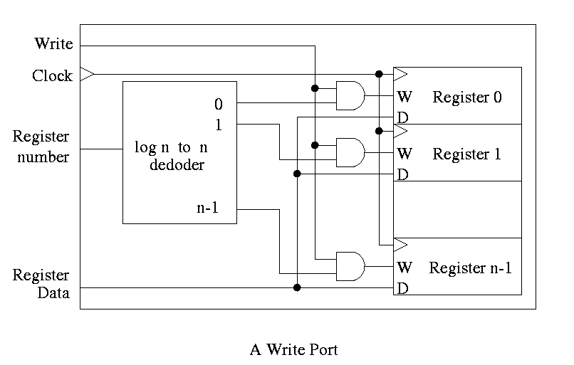
For writes use a decoder on register number to determine which
register to write. Note that 3 errors in the book's figure were fixed
- decoder is log n to n
- decoder outputs numbered 0 to n-1 (NOT n)
- clock is needed
The idea is to gate the write line with the output of the decoder. In
particular, we should perform a write to register r this cycle providing
- Recall that the inputs to a register are W, the write line, D the
data to write (if the write line is asserted) and the clock.
- The clock to each register is simply the clock input to the
register file.
- The data to each register is simply the write data to the register file.
- The write line to each register is unique
- The register number is fed to a decoder.
- The rth output of the decoder is asserted if r is the
specified register.
- Hence we wish to write register r if
- The write line to the register file is asserted
- The rth output of the decoder is asserted
- Bingo! We just need an and gate.

Homework: 20
SRAMS and DRAMS
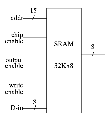
- External interface is below
- (Sadly) we will not look inside. Following is unofficial
- Conceptually like a register file but can't use the
implementation above for a large memory because there would be
too many wires and the muxes would be too big.
- Two stage decode
- Tri-state buffers instead of mux for SRAM. Hence I was
fibbing when I said that signals always have a 1 or 0.
However, we will not use tristate logic (will use muxes the
way we build them
- DRAM latches whole row but outputs only one (or a few)
column(s)
- So can speed up access to elts in same Row
- Merged DRAM + CPU a modern hot topic
- Error Correction (Omitted)

Note:
There are other kinds of flip-flops T, J-K. Also one could learn
about excitation tables for each. We will not cover this
material (H&P doesn't either). If interested, see Mano
Counters
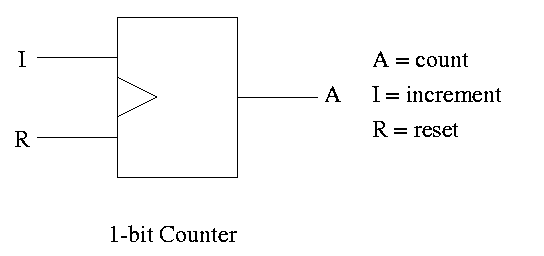
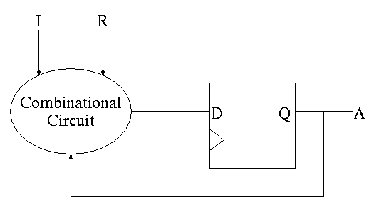
A counter
counts (naturally). The counting is done in binary.

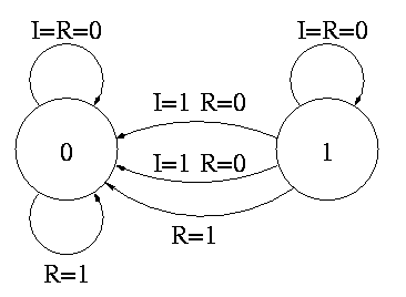
Let's look at the state transition diagram for A, the output of a
1-bit counter.

We need one flop and a combinatorial circuit.

The flop producing A is often itself called A and the D input to this
flop is called DA (really D sub A).
Current      Next ||
   A    I R   A   || DA <-- i.e. to what must I set DA
------------------++--      in order to
   0    0 0   0   || 0      get the desired Next A for
   1    0 0   1   || 1      the next cycle
   0    1 0   1   || 1
   1    1 0   0   || 0
   x    x 1   0   || 0
But this table (without Next A) is the truth table for the
combinatorial circuit.
A I R  || DA
-------++--
0 0 0  || 0
1 0 0  || 1
0 1 0  || 1
1 1 0  || 0
x x 1  || 0

DA = R' (A XOR I)
