There is a web page for the course. You can find it from my home page.
Text is Hennessy and Patterson ``Computer Orgaiization and Design The Hardware/Software Interface''.
I make a distinction between homework and labs.
Labs are
Upper left board for assignments and announcements.
Homework: Read B1
Homework: Read B2 Digital ==> Discrete
Primarily (but NOT exclusively) binary at the hardware level
Use only two voltages -- high and low
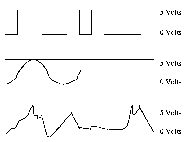
Since this is not an engineering course, we will ignore these issues and assume square waves.
In English digital (think digit, i.e. finger) => 10, but not in computers
Bit = Binary digIT
Instead of saying high voltage and low voltage, we say true and false or 1 and 0 or asserted and deasserted.
0 and 1 are called complements of each other.
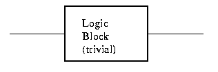
A logic block can be thought of as a black box that takes signals in and produces signals out. There are two kinds of blocks
We are doing combinational now. Will do sequential later (few lectures).
Since combinatorial logic has no memory, it is simply a function from its inputs to its outputs. A Truth Table has as columns all inputs and all outputs. It has one row for each possible set of input values and the output columns have the output for that input. Let's start with a really simple case a logic block with one input and one output.
There are two columns (1 + 1) and two rows (2**1).
In  Out
0   ?
1   ?
How many different truth tables are there for one in and one out?
Just 4: the constant functions 1 and 0, the identity, and an inverter (pictures in a few minutes). There were two `?'s in the above table each can be a 0 or 1 so 2**2 possibilities.
OK. Now how about two inputs and 1 output.
Three columns (2+1) and 4 rows (2**2).
In1 In2  Out
0   0    ?
0   1    ?
1   0    ?
1   1    ?
How many are there? It is just how many ways can you fill in the output entries. There are 4 output entries so answer is 2**4=16.
How about 2 in and 8 out?
3 in and 8 out?
n in and k out?
Gets big fast!
Certain logic functions (i.e. truth tables) are quite common and familiar.
We use a notation that looks like algebra to express logic functions and expressions involving them.
The notation is called Boolean algebra in honor of George Boole.
A Boolean value is a 1 or a 0.
A Boolean variable takes on Boolean values.
A Boolean function takes in boolean variables and produces boolean values.
Homework: Consider the Boolean function of 3 boolean vars that is true if and only if exactly 1 of the three variables is true. Draw the TT.
Some manipulation laws. Remember this is Boolean ALGEBRA.
Identity:
Inverse:
Both + and . are commutative so don't need as much as I wrote
The name inverse law is somewhat funny since you Add the inverse and get the identity for Product or Multiply by the inverse and get the identity for Sum.
Associative:
Due to associative law we can write A.B.C since either order of evaluation gives the same answer.
Often elide the . so the product associative law is A(BC)=(AB)C.
Distributive:
How does one prove these laws??
Homework: Do the second distributive law.
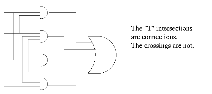
Let's do (on the board) the examples on pages B-5 and B-6. Consider a logic function with three inputs A, B, and C; and three outputs D, E, and F defined as follows: D is true if at least one input is true, E if exactly two are true, and F if all three are true. (Note that by if we mean if and only if.
Draw the truth table.
Show the logic equations
The first way we solved part E shows that any logic function can be written using just AND, OR, and NOT. Indeed, it is in a nice form. Called two levels of logic, i.e. it is a sum of products of just inputs and their compliments.
DeMorgan's laws:
You prove DM laws with TTs. Indeed that is ...
Homework: B.6 on page B-45
Do beginning of HW on the board.
With DM we can do quite a bit without resorting to TTs. For example one can show that the two expressions for E on example above (page B-6) are equal. Indeed that is
Homework: B.7 on page B-45
Do beginning of HW on board.
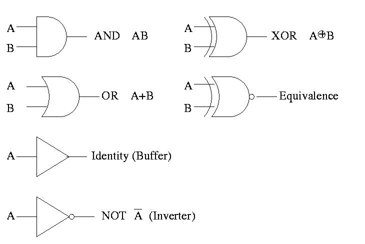
Gates implement basic logic functions: AND OR NOT XOR Equivalence
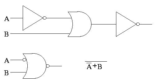
Show why the picture is equivalence, i.e (A XOR B)' is AB + A'B'
(A XOR B)' =
(A'B+AB')' =
(A'B)' (AB')' =
(A''+B') (A'+B'') =
(A + B') (A' + B) =
AA' + AB + B'A' + B'B =
0   + AB + B'A' + 0 =
AB + A'B'
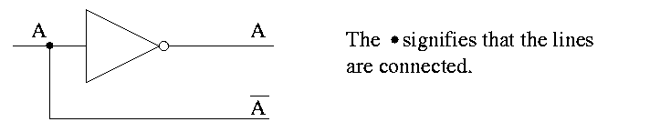
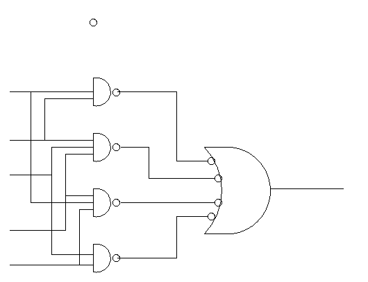
Often omit the inverters and draw the little circles at the input or
output of the other gates (AND OR). These little circles are
sometimes called bubbles.
This explains why inverter is drawn as a buffer with a bubble.
Homework: B.2 on page B-45 (I previously did the first part of this homework).
Homework: Consider the Boolean function of 3 boolean vars (i.e. a three input function) that is true if and only if exactly 1 of the three variables is true. Draw the TT. Draw the logic diagram with AND OR NOT. Draw the logic diagram with AND OR and bubbles.
We have seen that any logic function can be constructed from AND OR NOT. So this triple is called universal.
Are there any pairs that are universal? Could it be that there is a single function that is universal? YES!
NOR (NOT OR) is true when OR is false. Do TT.
NAND (NOT AND) is true when AND is false. Do TT.
Draw two logic diagrams for each, one from definition and equivalent one with bubbles.
Theorem A 2-input NOR is universal and A 2-input NAND is universal.
Proof
We must show that you can get A', A+B, and AB using just a two input NOR.
Homework: Show that a 2-input NAND is universal.
Can draw NAND and NOR each two ways (because (AB)' = A' + B')
We have seen how to get a logic function from a TT. Indeed we can get one that is just two levels of logic. But it might not be the simplest possible. That is we may have more gates than necessary.
Trying to minimize the number of gates is NOT trivial. Mano covers this in detail. We will not cover it in this course. It is not in H&P. I actually like it but must admit that it takes a few lectures to cover well and it not used so much since it is algorithmic and is done automatically by CAD tools.
Minimization is not unique, i.e. there can be two or more minimal forms.
Given A'BC + ABC + ABC'
Combine first two to get BC + ABC'
Combine last two to get A'BC + AB
Sometimes when building a circuit, you don't care what the output is for certain input values. For example, that input combination is cannot occur. Another example occurs when, for this combination of input values, a later part of the circuit will ignore the output of this part. These are called don't care outputs situations. Making use of don't cares can reduce the number of gates needed.
Can also have don't care inputs when , for certain values of a subset of the inputs, the output is already determined and you don't have to look at the remaining inputs. We will see a case of this in the very next topic, multiplexors.
Putting a circuit in disjunctive normal form (i.e. two levels of logic) means that every path from the input to the output goes through very few gates. In fact only two, an OR and an AND. Maybe we should say three since the AND can have a NOT (bubble). Theorticians call this number (2 or 3 in our case) the depth of the circuit. Se we see that every logic function can be implemented with small depth. But what about the width, i.e., the number of gates.
The news is bad. The parity function takes n inputs and gives TRUE if and only if the number of input TRUEs is odd. If the depth is fixed (say limited to 3), the number of gates needed for parity is exponential in n.
Homework: Read B.3.
Generic Homework: Read sections in book corresponding to the lectures.
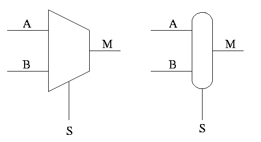
Often called a mux or a selector
Show equiv circuit with AND OR
Hardware if-then-else
    if S=0
        M=A
    else
        M=B
    endif
Can have 4 way mux (2 selector lines)
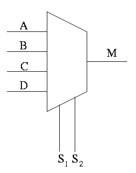
This is an if-then-elif-elif-else
   if S1=0 and S2=0
        M=A
    elif S1=0 and S2=1
        M=B
    elif S1=1 and S2=0
        M=C
    else -- S1=1 and S2=1
        M=D
    endif
Do a TT for 2 way mux. Redo it with don't care values.
Do a TT for 4 way mux with don't care values.
Homework: B-12. Assume you have constant signals 1 and 0 as well.
Sneaky way to see that NAND is universal.
Homework: Draw logic diagram
Homework:
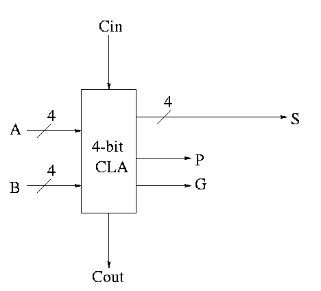
How about 4 bit adder ?
How about n bit adder ?
Idea is to make use of the algorithmic way you can look at a TT and produce a circuit diagram in the sums of product form.
Consider the following TT from the book (page B-13)
     A | B | C || D | E | F
     --+---+---++---+---+--
     O | 0 | 0 || 0 | 0 | 0
     0 | 0 | 1 || 1 | 0 | 0
     0 | 1 | 0 || 1 | 0 | 0
     0 | 1 | 1 || 1 | 1 | 0
     1 | 0 | 0 || 1 | 0 | 0
     1 | 0 | 1 || 1 | 1 | 0
     1 | 1 | 0 || 1 | 1 | 0
     1 | 1 | 1 || 1 | 0 | 1
Here is the circuit diagram for this truth table.
Here it is redrawn

Finally, it can be redrawn in a more abstract form.
When a PLA is manufactured all the connections have been specified. That is, a PLA is specific for a given circuit. It is somewhat of a misnomer since it is notprogrammable by the user
Homework: B.10 and B.11
Can also have a PAL or Programmable array logic in which the final dots are specified by the user. The manufacturer produces a ``sea of gates''; the user programs it to the desired logic function.
Homework: Read B-5
One way to implement a mathematical (or C) function (without side effects) is to perform a table lookup.
A ROM (Read Only Memory) is the analogous way to implement a logic function.
Important: The ROM is does not have state. It is still a combinational circuit. That is, it does not represent ``memory''. The reason is that once a ROM is manufactured, the output depends only on the input.
A PROM is a programmable ROM. That is you buy the ROM with ``nothing'' in its memory and then before it is placed in the circuit you load the memory, and never change it.
An EPROM is an erasable PROM. It costs more but if you decide to change its memory this is possible (but is slow).
``Normal'' EPROMs are erased by some ultraviolet light process. But EEPROMs (electrically erasable PROMS) are faster and are done electronically.
All these EPROMS are erasable not writable, i.e. you can't just change one bit.
A ROM is similar to PLA
Example
Full truth table
     A   B   C || D   E   F
     ----------++----------
     0   0   0 || 0   0   0
     0   0   1 || 1   0   1
     0   1   0 || 0   1   1
     0   1   1 || 1   1   0
     1   0   0 || 1   1   1
     1   0   1 || 1   1   0
     1   1   0 || 1   1   0
     1   1   1 || 1   1   1
Put in the output don't cares
     A   B   C || D   E   F
     ----------++----------
     0   0   0 || 0   0   0
     0   0   1 || 1   0   1
     0   1   0 || 0   1   1
     0   1   1 || 1   1   X
     1   0   0 || 1   1   X
     1   0   1 || 1   1   X
     1   1   0 || 1   1   X
     1   1   1 || 1   1   X
Now do the input don't cares
     A   B   C || D   E   F
     ----------++----------
     0   0   0 || 0   0   0
     0   0   1 || 1   0   1
     0   1   0 || 0   1   1
     X   1   1 || 1   1   X
     1   X   X || 1   1   X
These don't cares are important for logic minimization. Compare the number of gates needed for the full TT and the reduced TT. There are techniques for minimizing logic, but we will not cover them.
Why do we want to have state?
Assume you have a real OR gate. Assume the two inputs are both zero for an hour. At time t one input becomes 1. The output will OSCILLATE for a while before settling on exactly 1. We want to be sure we don't look at the answer before its ready.
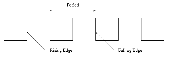
Frequency and period
Edges
Now we are going to add state elements to the combinational circuits we have been using previously.
Remember that a combinational/combinatorial circuits has its outpus determined by its input, i.e. combinatorial circuits do not contain state.
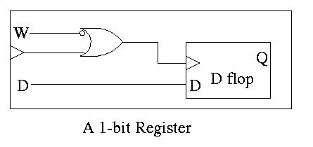
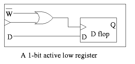
Reading and writing State Elements.
State elements include state (naturally).
We want edge-triggered clocked memory and will only use edge-triggered clocked memory in our designs. However we get there by stages. We first show how to build unclocked memory; then using unclocked memory we build level-sensitive clocked memory; finally from level-sensitive clocked memory we build edge-triggered clocked memory.
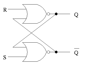
S-R latch (set-reset)
The S-R latch defined above is not clocked memory. Unfortunately the terminology is not perfect.
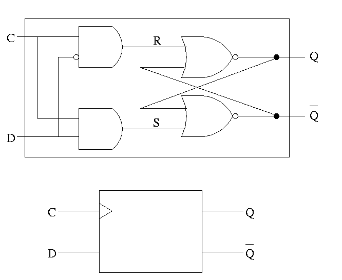
For both flip-flops and latches the output equals the value stored in the structure. Both have an input and an output (and the complemented output) and a clock input as well. The clock determines when the internal value is set to the current input. For a latch, the change occurs whenever the clock is asserted (level sensitive). For a flip-flop, the change only occurs during the active edge.
The D is for data
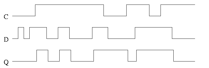
In the traces below notice how the output follows the input when the clock is high and remains constant when the clock is low. We assume the stored value is initially low.
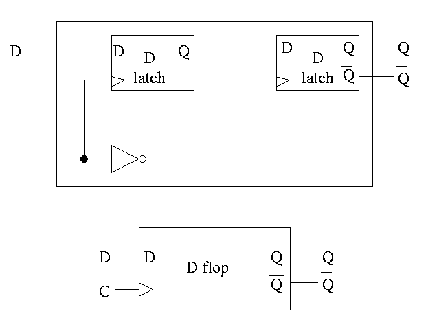
This was our goal. We now have an edge-triggered, clocked memory.
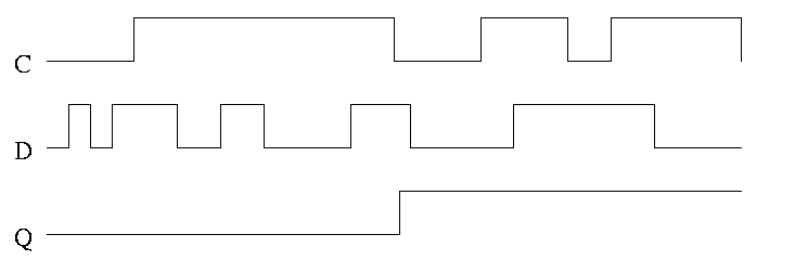
Note how much less wiggly the output is with the master-slave flop than before with the transparent latch. As before we are assuming the output is initially low.
Homework: Try moving the inverter to the other latch What has changed?
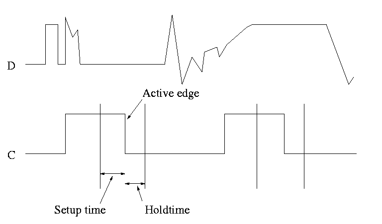
This picture shows the setup and hold times discussed above. It is crucial when building circuits with flip flops that D is stable during the interval between the setup and hold times. Note that D is wild outside the critical interval, but that is OK.
Homework: B.18
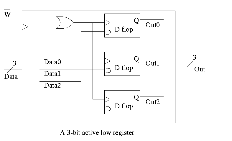
Set of registers each numbered
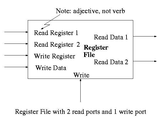
To read just need mux from register file to select correct register.
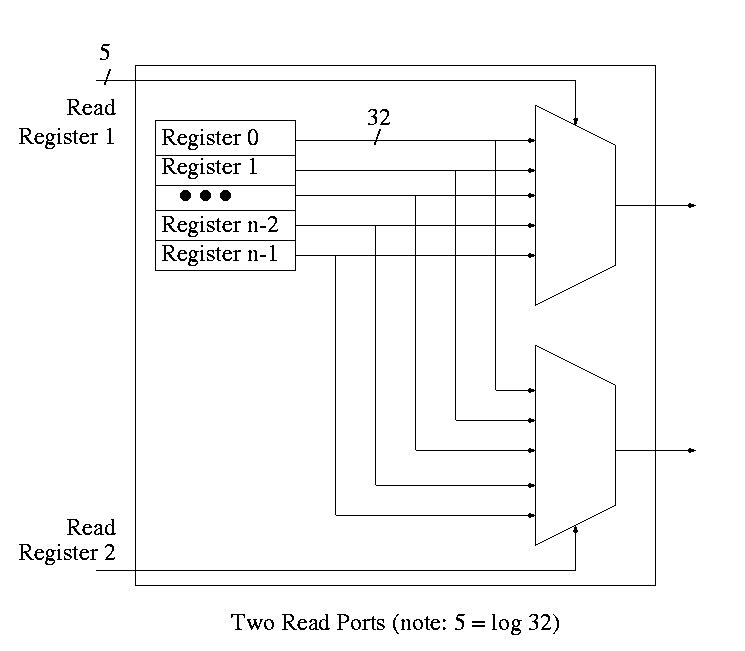
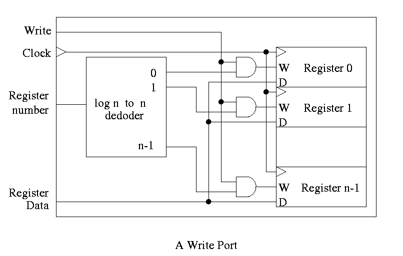
For writes use a decoder on register number to determine which register to write. Note that 3 errors in the book's figure were fixed
The idea is to gate the write line with the output of the decoder. In particular, we should perform a write to register r this cycle providing
Homework: 20
Note: There are other kinds of flip-flops T, J-K. Also one could learn about excitation tables for each. We will not cover this material (H&P doesn't either). If interested, see Mano
A counter counts (naturally). The counting is done in binary.
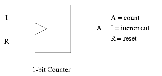
Let's look at the state transition diagram for A, the output of a 1-bit counter.
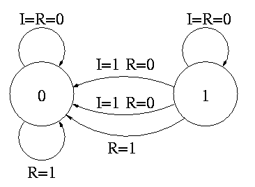
We need one flop and a combinatorial circuit.
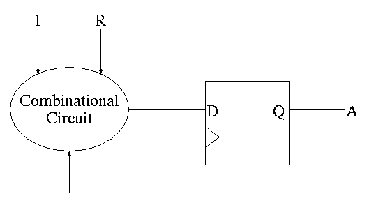
The flop producing A is often itself called A and the D input to this flop is called DA (really D sub A).
Current      Next ||
   A    I R   A   || DA <-- i.e. to what must I set DA
------------------++--      in order to
   0    0 0   0   || 0      get the desired Next A for
   1    0 0   1   || 1      the next cycle
   0    1 0   1   || 1
   1    1 0   0   || 0
   x    x 1   0   || 0
But this table (without Next A) is the truth table for the combinatorial circuit.
A I R  || DA
-------++--
0 0 0  || 0
1 0 0  || 1
0 1 0  || 1
1 1 0  || 0
x x 1  || 0

DA = R' (A XOR I)
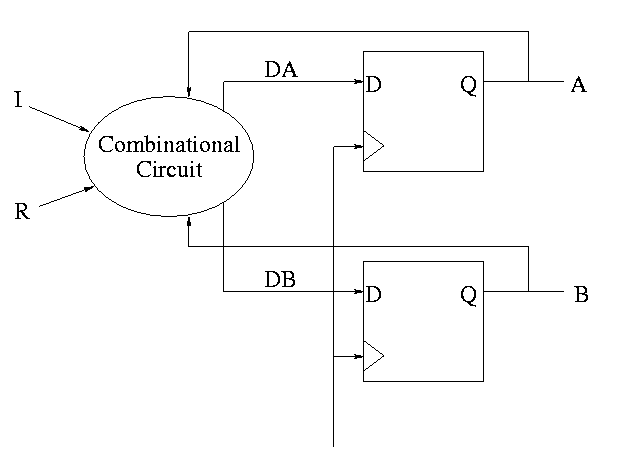
How about a two bit counter.
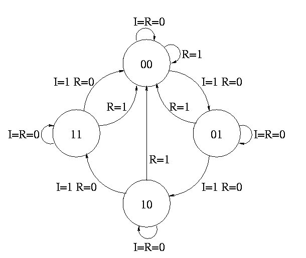
To determine the combinationatorial circuit we could preceed as before
Current      Next ||
  A B   I R  A B  || DA DB
------------------++------
This would work but we can instead think about how a counter works and see that.
DA = R'(A XOR I)
DB = R'(B XOR AI)
Homework: 23
Skipped
Skipped
Homework:
READ chapter 1. Do 1.1 -- 1.26 (really one matching question)
Do 1.27 to 1.44 (another matching question),
1.45 (and do 7200 RPM and 10,000 RPM),
1.46, 1.50
Homework: Read sections 3.1 3.2 3.3
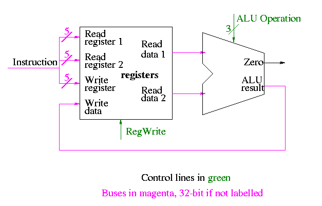
Register file
Homework: 3.2
    op    rs    rt    rd    shamt  funct
    6     5     5     5      5      6
The fields are quite consistent
Example: add $1,$2,$3
    op    rs    rt   address
    6     5     5     16
lw/sw $1,addr($2)
RISC-like properties of the MIPS architecture
    stl $1,$5,$8
    bne $1,$0,L
    stl $1,$8,$5
    beq $1,$0,L
    stl $1,$8,$5
    bne $1,$0,L
    stl $1,$5,$8
    beq $1,$0,L
Note: Please do not make the mistake of thinking that
    stl $1,$5,$8
    beq $1,$0,L
is the same as
    stl $1,$8,$5
    bne $1,$0,L
The negation of X < Y is not Y < X
Homework: 3.12-3.17
        op   address
        6     26
addi $1,$2,100
Why is there no subi?
Ans: Make the immediate operand negative.
slti $1,$2,50
Homework: 3.1, 3.3-3.7, 3.9, 3.18, 3.37 (for fun)
Homework: 4.1-4.9
MIPS uses 2s complement (just like 8086)
To form the 2s complement (of 0000 1111 0000 1010 0000 0000 1111 1100)
Need comparisons for signed and unsigned.
Just like slt and slti but the comparison is unsigned.
To add two (signed) numbers just add them. That is don't treat the sign bit special.
To subtract A-B, just take the 2s complement of B and add.
An overflow occurs when the result of an operatoin cannot be represented with the available hardware. For MIPS this means when the result does not fit in a 32-bit word.
  11111111111111111111111111111111   (32 ones is -1)
+ 11111111111111111111111111111111
----------------------------------
 111111111111111111111111111111110   Now discard the carry out

  11111111111111111111111111111110   this is -2
Operation  Operand A  Operand B  Result
   A+B       >= 0        >= 0      < 0
   A+B        < 0         < 0     >= 0
   A-B       >= 0         < 0      < 0
   A-B        < 0        >= 0     >= 0
> I have a question about the first lab; I'm not sure how we
> would implement a mux, would a series of if-else
> statements be an acceptable option?

No.  But that is a good question.  if-then-elif...-else
would be a FUNCTIONAL simulation.  That is you are
simulating what the mux does but not HOW it does it.  For a
gate level simulation, you need to implement the mux in
terms of AND, NOT, OR, XOR and then write code link
Fulladder.c

The implementation of a two way mux in terms of AND OR NOT
is figure B.4 on page B-9 of the text.  You need to do a 3
way mux.
Homework: (for fun) prove this last statement (4.29)
These add and subtract the same the same was as add and sub, but do not signal overflow
No surprises.
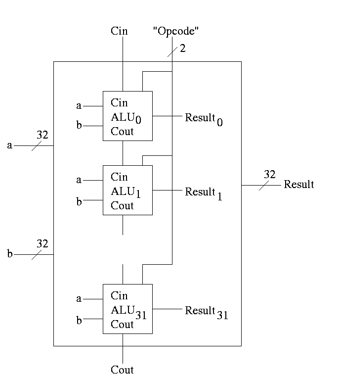
First goal is 32-bit AND, OR, and addition
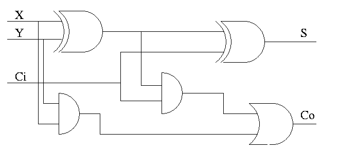
Recall we know how to build a full adder. Will draw it as
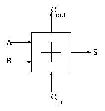
With this adder, the ALU is easy.
32-bit version is simple.
First goal accomplished.
How about subtraction?
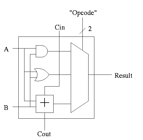
1-bit ALU with ADD, SUB, AND, OR is

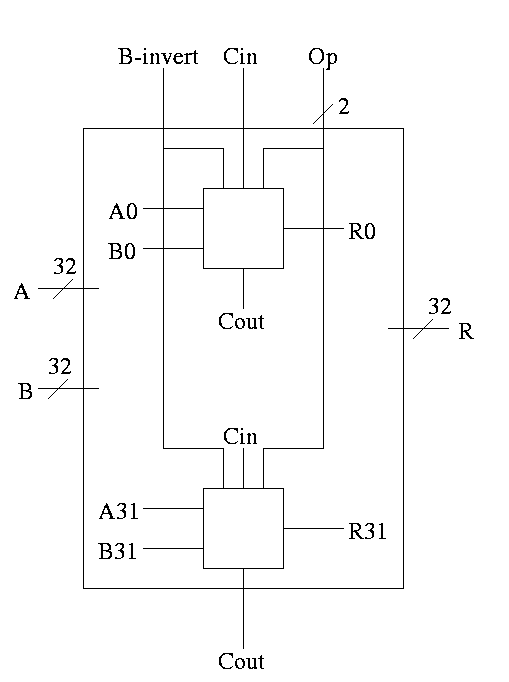
For subtraction set Binvert and Cin.
32-bit version is simply a bunch of these.
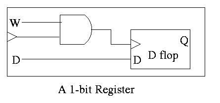
Write a procedure for each logic box with the following properties.
Handout: FullAdder.c and FourBitAdder.c.
Lab 1: Do the equivalent for 1-bit-alu (without subtraction). This is easy. Lab 2 will be similar but for a more sophisticated ALU.
Extra requirements for MIPS alu:
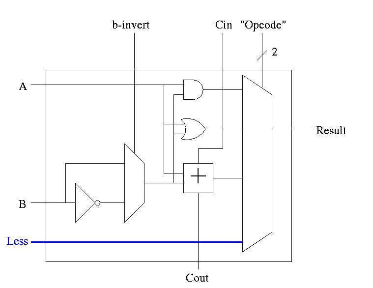
The Final Result is
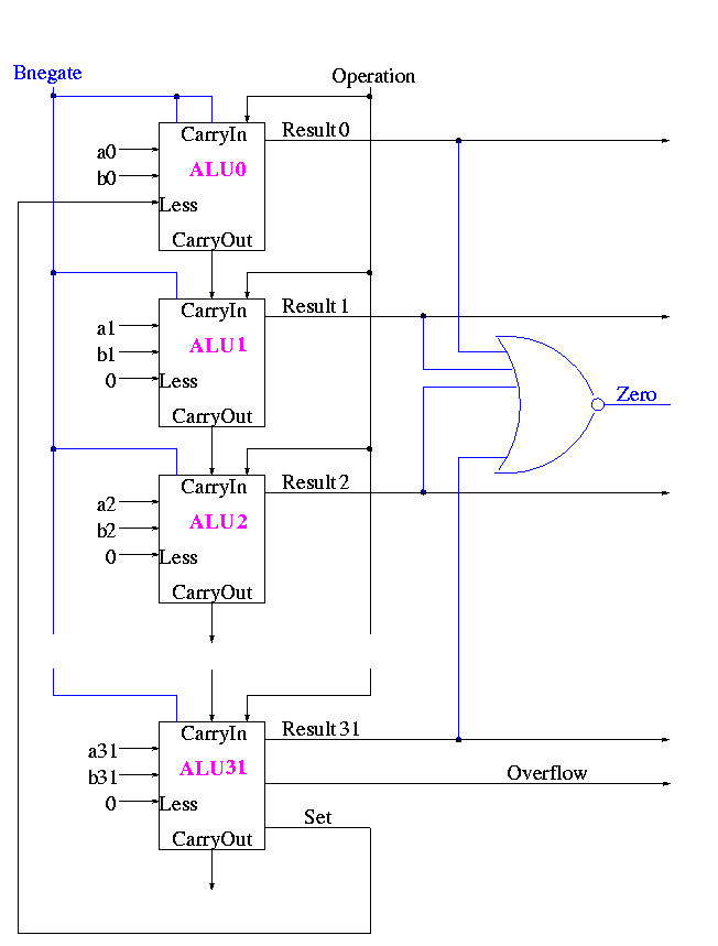
Symbol for the alu is
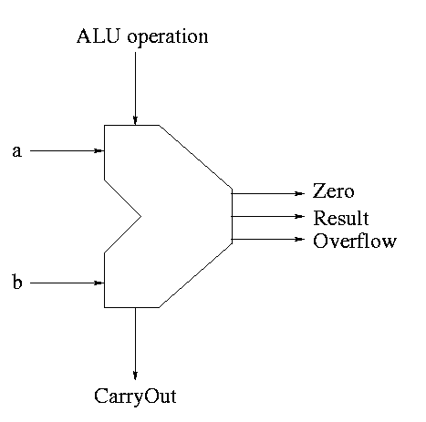
What are the control lines?
What functions can we perform?
What (3-bit) values for the control lines do we need for each function?
| and | 0 | 00 |
| or | 0 | 01 |
| add | 0 | 10 |
| sub | 1 | 10 |
| slt | 1 | 11 |
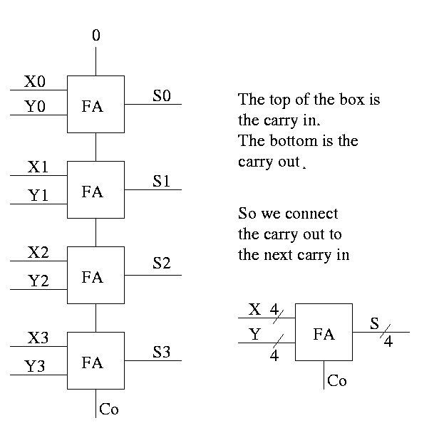
Adders
We did a ripple adder
We will now do the carry lookahead adder, which is much faster, especially for many bit (e.g. 64 bit) addition.
For each bit we can in one gate delay calculate
    generate a carry    gi = ai bi

    propogate a carry   pi = ai+bi
H&P give a plumbing analogue for generate and propogate.
Given the generates and propogates, we can calculate all the carries for a 4-bit addition (recall that c0=Cin is an input) as follows
c1 = g0 + p0 c0

c2 = g1 + p1 c1 = g1 + p1 g0 + p1 p0 c0

c3 = g2 + p2 c2 = g2 + p2 g1 + p2 p1 g0 + p2 p1 p0 c0

c4 = g3 + p3 c3 = g3 + p3 g2 + p3 p2 g1 + p3 p2 p1 g0 + p3 p2 p1 p0 c0
Thus we can calculate c1 ... c4 in just two additional gate delays (where we assume one gate can accept upto 5 inputs). Since we get gi and pi after one gate delay, the total delay for calculating all the carries is 3 (this includes c4=CarryOut)
Each bit of the sum si can be calculated in 2 gate delays given ai, bi, and ci. Thus 5 gate delays after we are given a, b and CarryIn, we have calculated s and CarryOut
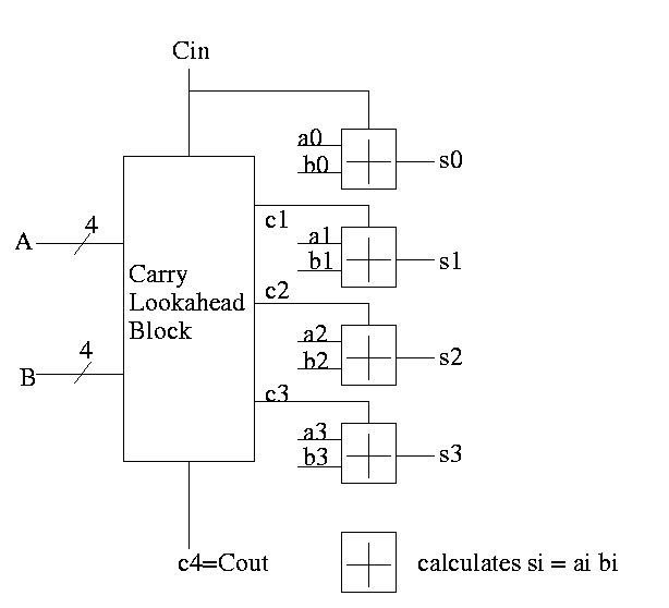
So for 4-bit addition the faster adder takes time 5 and the slower adder time 8.
Now we want to put four of these together to get a fast 16-bit adder. Again we are assuming a gate can accept upto 5 inputs. It is important that the number of inputs per gate does not grow with the size of the numbers to add. If the technology available supplies only 4-input gates, we would use groups of 3 bits rather than four.
We start by determining ``supergenerate'' and ``superpropogate'' bits. The super propogate indicates whether the 4-bit adder constructed above generates a CarryOut or propogates a CarryIn to a CarryOut
P0 = p3 p2 p1 p0          Does the low order 4-bit adder
                          propogate a carry?
P1 = p7 p6 p5 p4

P2 = p11 p10 p9 p8

P3 = p15 p14 p13 p12      Does the high order 4-bit adder
                          propogate a carry?


G0 = g3 + p3 g2 + p3 p2 g1 + p3 p2 p1 g0        Does low order 4-bit
                                                adder generate a carry
G1 = g7 + p7 g6 + p7 p6 g5 + p7 p6 p5 g4

G2 = g11 + p11 g10 + p11 p10 g9 + p11 p10 p9 g8

G3 = g15 + p15 g14 + p15 p14 g13 + p15 p14 p13 g12


C1 = G0 + P0 c0

C2 = G1 + P1 C1 = G1 + P1 G0 + P1 P0 c0

C3 = G2 + P2 C2 = G2 + P2 G1 + P2 P1 G0 + P2 P1 P0 c0

C4 = G3 + P3 C3 = G3 + P3 G2 + P3 P2 G1 + P3 P2 P1 G0 + P3 P2 P1 P0 c0
From these C's you just need to do a 4-bit CLA since the C's are the CarryIns for each group of 4-bits out of the 16-bits.
How long does this take, again assuming 5 input gates?
Some pictures follow.
Take our original picture of the 4-bit CLA and collapse the details so it looks like.
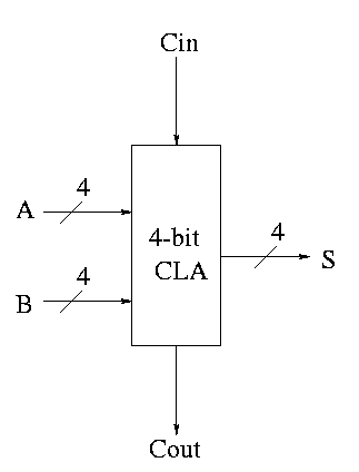
Next include the logic to calculate P and G
Now put four of these with a CLA block (to calculate C's from P's, G's and Cin) and we get a 16-bit CLA. Note that we do not use the Cout from the 4-bit CLAs.
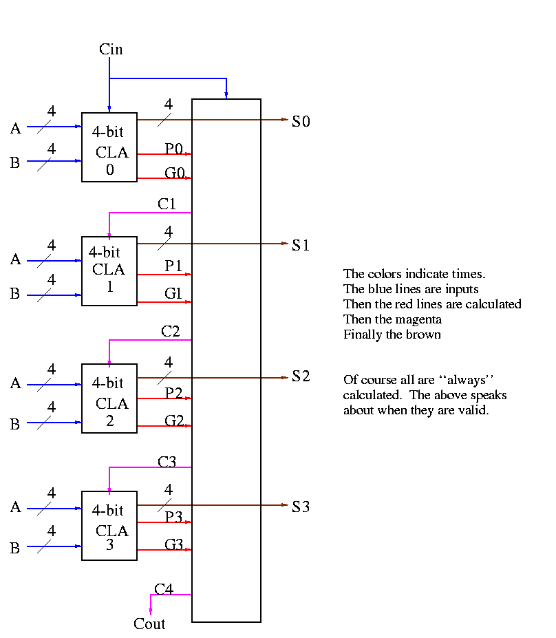
Note that the tall skinny box is general. It takes 4 Ps 4Gs and Cin and calculates 4Cs. The Ps can be propogates, superpropogates, superduperpropogates, etc. That is, you take 4 of these 16-bit CLAs and the same tall skinny box and you get a 64-bit CLA.
Homework: 4.44, 4.45
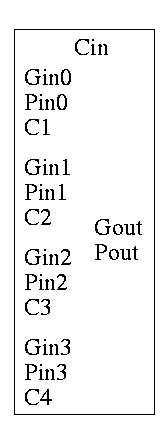
As noted just above the tall skinny box is useful for all size CLAs. To expand on that point and to review CLAs, let's redo CLAs with the general box.
Since we are doing 4-bits at a time, the box takes 9=2*4+1 input bits and produces 6=4+2 outputs
C1 = G0 + PO Cin
C2 = G1 + P1 G0 + P1 P0 Cin
C3 = G2 + P2 G1 + P2 P1 G0 + P2 P1 P0 Cin
C4 = G3 + P3 G2 + P3 P2 G1 + P3 P2 P1 G0 + P3 P2 P1 P0 Cin

Gout = G3  +  P3 G2  +  P3 P2 G1  +  P3 P2 P1 Go
Pout = P3 P2 P1 P0
A 4-bit adder is now
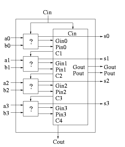
What does the ``?'' box do?
Now take four of these 4-bit adders and use the identical CLA box to get a 16-bit adder
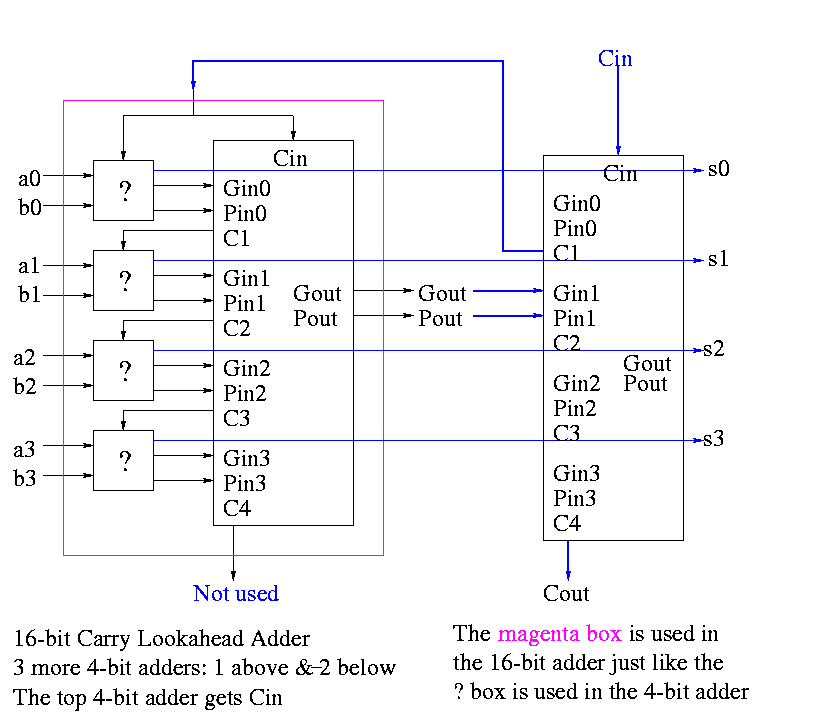
Four of these 16-bit adders with the identical CLA box to gives a 64-bit adder.
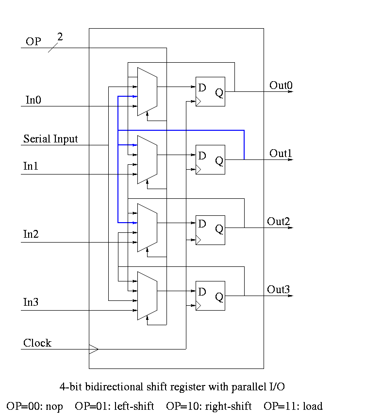
Homework: A 4-bit shift register initially contains 1101. It is shifted six times to the right with the serial input being 101101. What is the contents of the register after each shift.
Homework: Same register, same init condition. For the first 6 cycles the opcodes are left, left, right, nop, left, right and the serial input is 101101. The next cycle the register is loaded (in parallel) with 1011. The final 6 cycles are the same as the first 6. What is the contents of the register after each cycle?
    product <- 0
    for i = 0 to 31
        if LOB of multiplier = 1
            product = product + multiplicand
        shift multiplicand left 1 bit
        shift multiplier right 1 bit
Do on board 4-bit addition (8-bit registers) 1100 x 1101
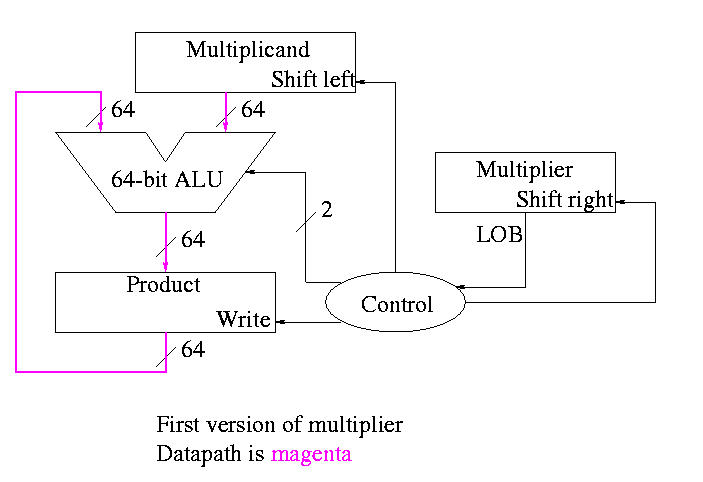
What about the control?
This works!
but, when compared to the better solutions to come, is wasteful of
resourses and hence is
The product register must be 64 bits since the product is 64 bits
Why is multiplicand register 64 bits?
Why is ALU 64-bits?
POOF!! ... as the smoke clears we see an idea.
We can solve both problems at once
This results in the following algorithm
    product <- 0
    for i = 0 to 31
        if LOB of multiplier = 1
            (serial_in, product[32-63]) <- product[32-63] + multiplicand
        shift product right 1 bit
        shift multiplier right 1 bit
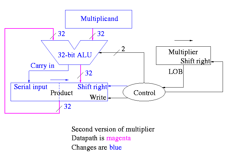
What about control
Redo same example on board
A final trick (``gate bumming'', like code bumming of 60s)
    product[0-31] <- multiplier
    for i = 0 to 31
        if LOB of product = 1
            (serial_in, product[32-63]) <- product[32-63] + multiplicand
        shift product right 1 bit
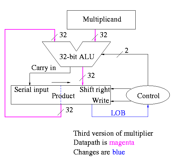
Control again boring
Redo same example on board
The above was for unsigned 32-bit multiplication
For signed multiplication
There are faster multipliers, but we are not covering them.
We are skiping division.
We are skiping floating point.
Homework: Read 4.11 ``Historical Perspective''.
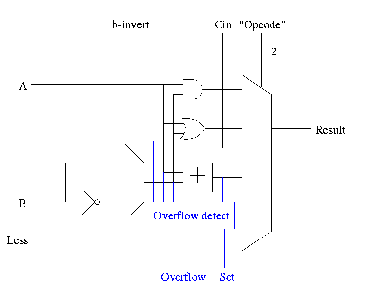
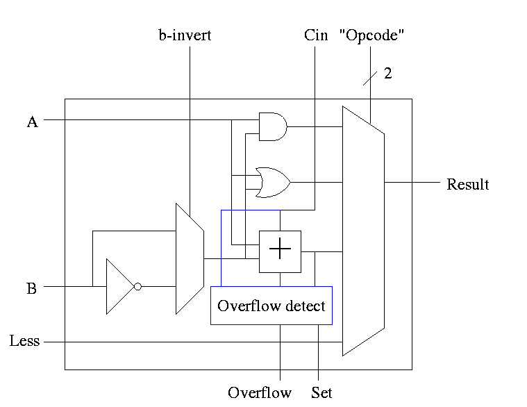
Lab 2. Due in three weeks. Modify lab 1 to deal with sub, slt, zero detect, overflow. Also lab 2 is to be 32 bits. That is, Figure 4.18.
Go over the exam.
Homework: Start Reading Chapter 5.
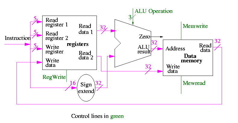
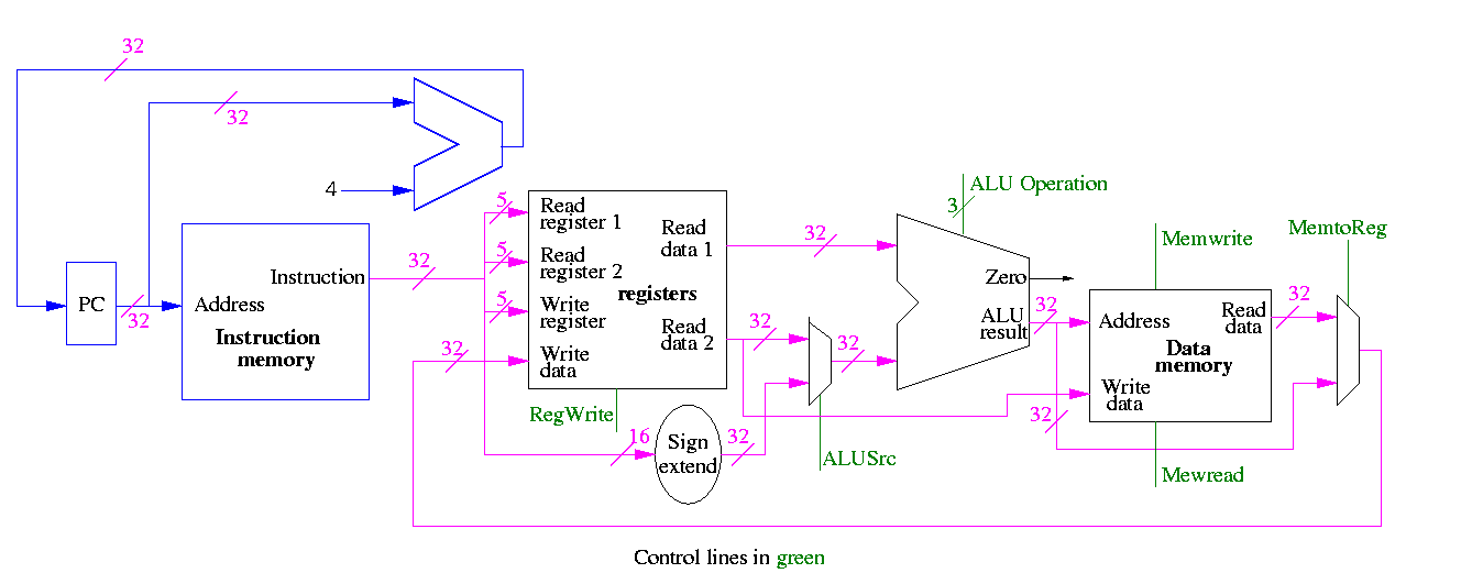
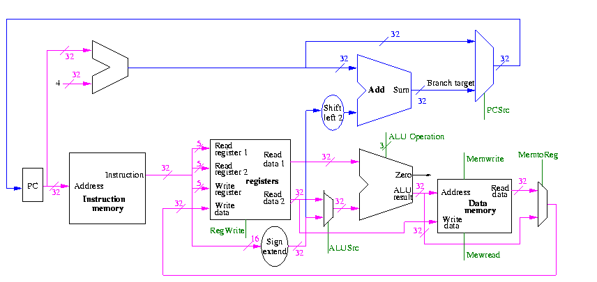
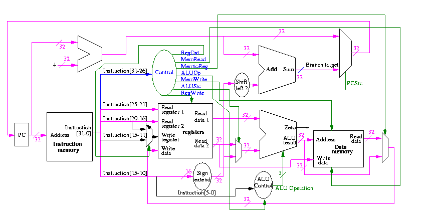
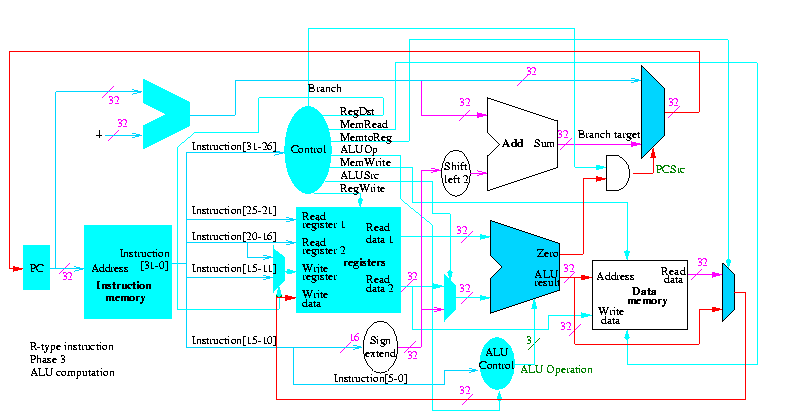
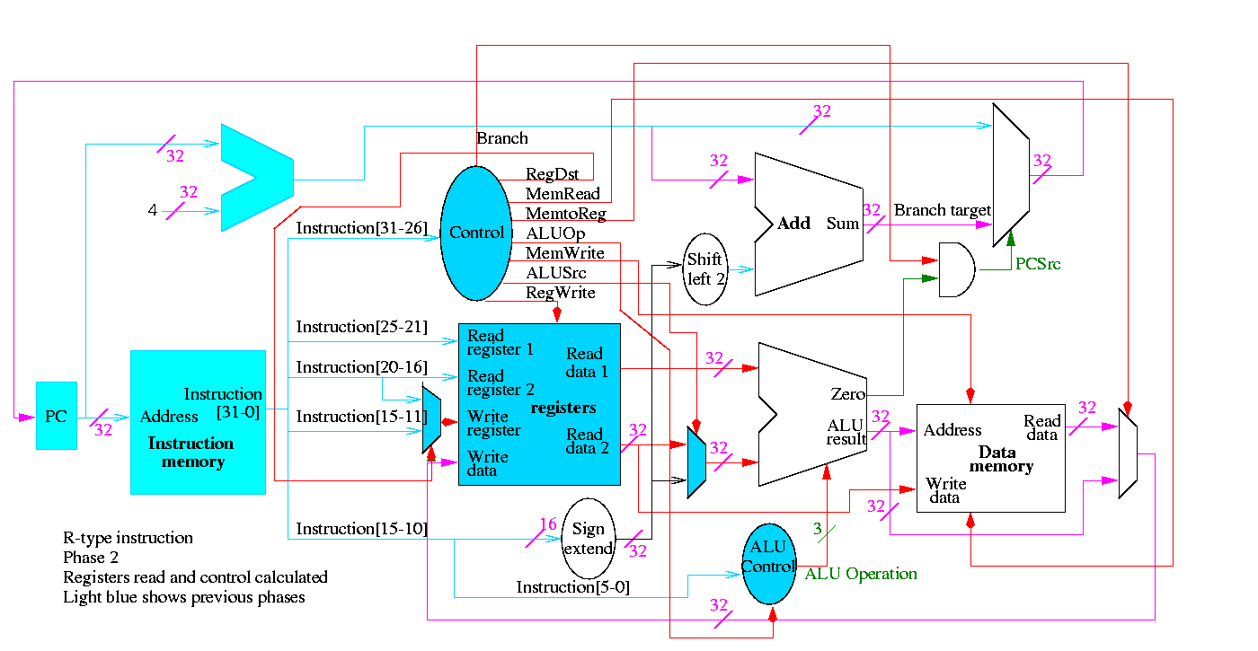
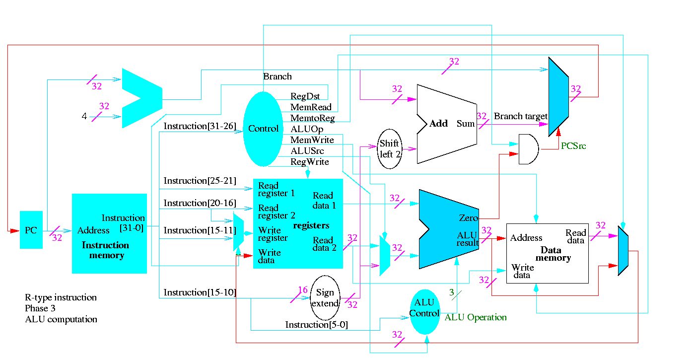
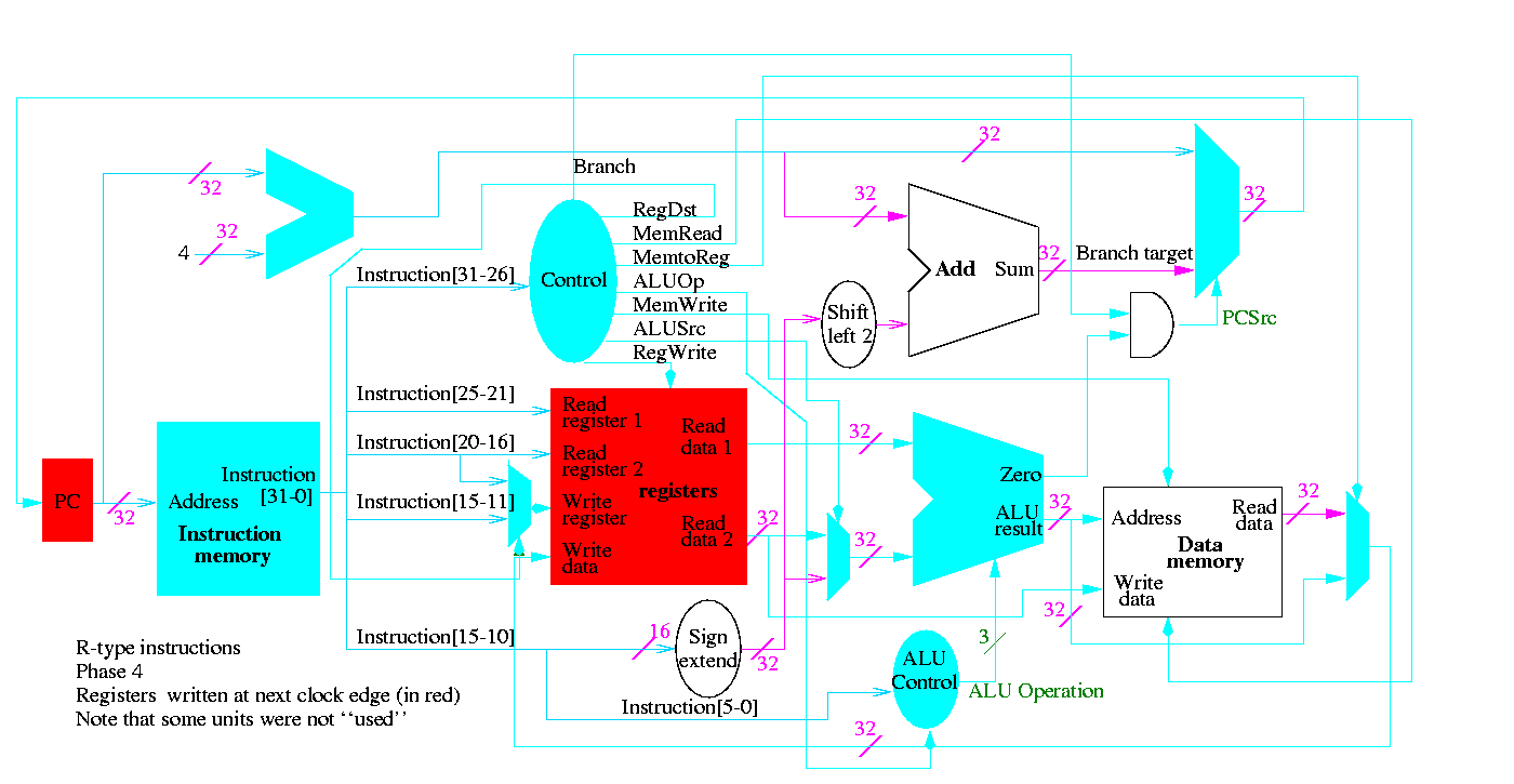
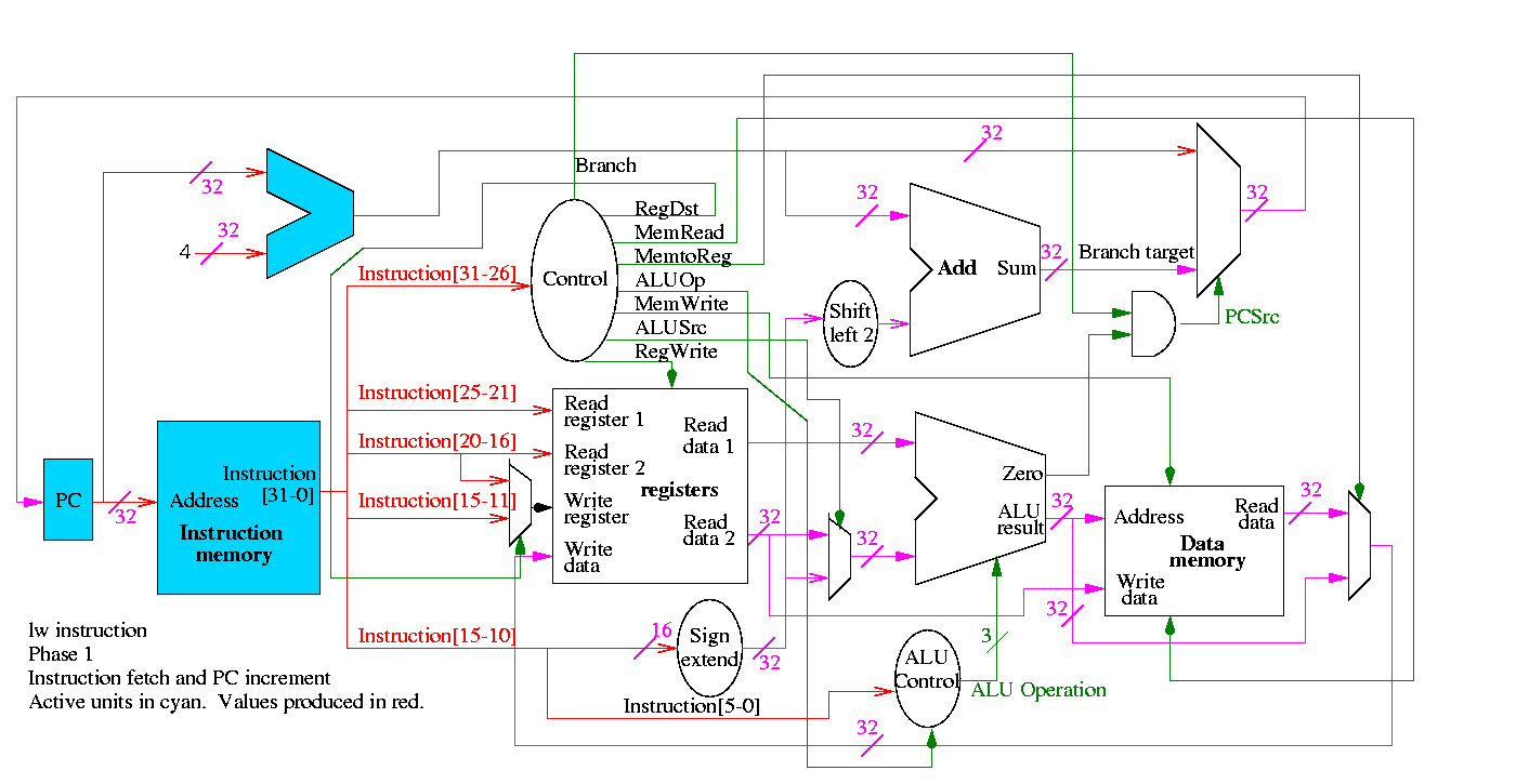
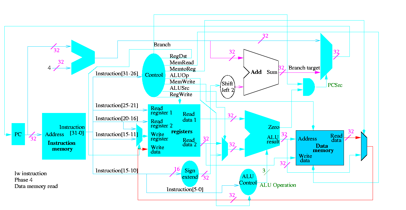
We are going to build the MIPS processor
Figure 5.1 redrawn below shows the main idea
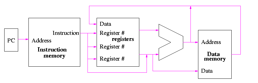
Note that the instruction gives the three register numbers as well as an immediate value to be added.
Let's begin doing the pieces in more detail.
We are ignoring branches for now.
lw  $r,disp($s)
sw  $r,disp($s)
There is a cheat here.
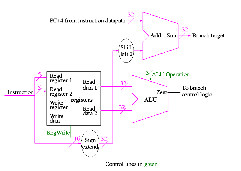
Compare two registers and branch if equal
We will just put the pieces together and then figure out the control lines that are needed and how to set them. We are not now worried about speed.
We are assuming that the instruction memory and data memory are separate. So we are not permitting self modifying code. We are not showing how either memory is connected to the outside world (i.e. we are ignoring I/O).
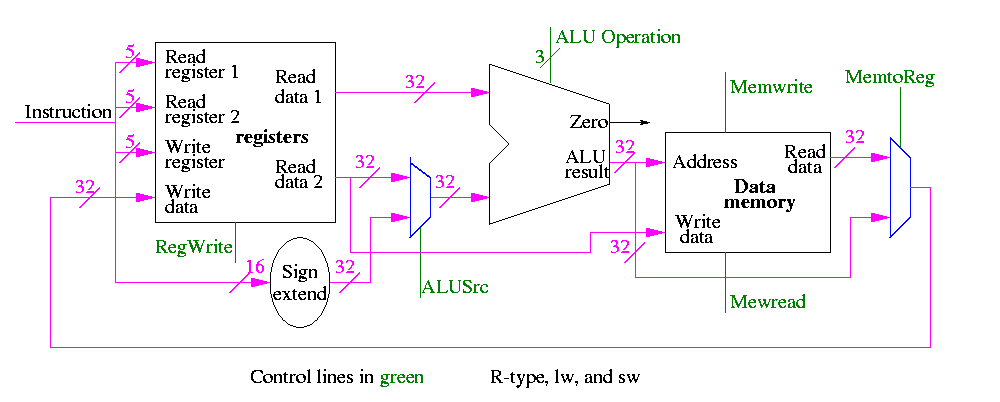
We have to use the same register file with all the pieces since when a load changes a register a subsequent R-type instruction must see the change, when an R-type instruction makes a change the lw/sw must see it (for loading or calculating the effective address, etc.
We could use separate ALUs for each type but it is easy not to so we will use the same ALU for all. We do have a separate adder for incrementing the PC.
The problem is that some inputs can come from different sources.
We will deal with the first two now by using a mux for each. We will deal with the third shortly by (surprise) using a mux.
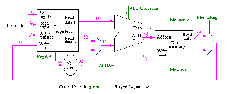
This is quite easy

We need to have an ``if stmt'' for PC (i.e., a mux)
Homework:
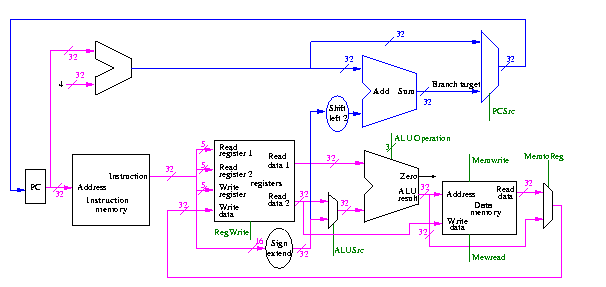
We start with our last figure, which shows the data path and then add the missing mux and show how the instruction is broken down.
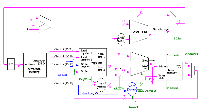
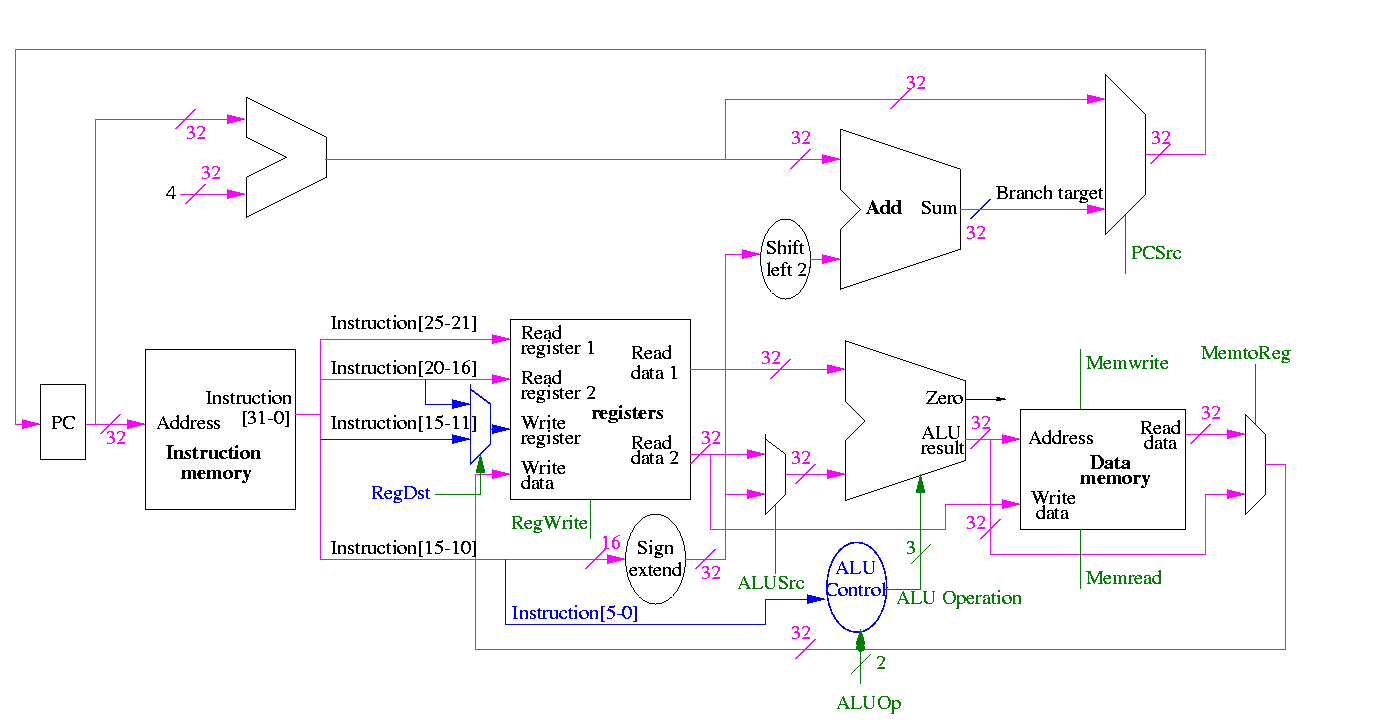
We need to set the muxes.
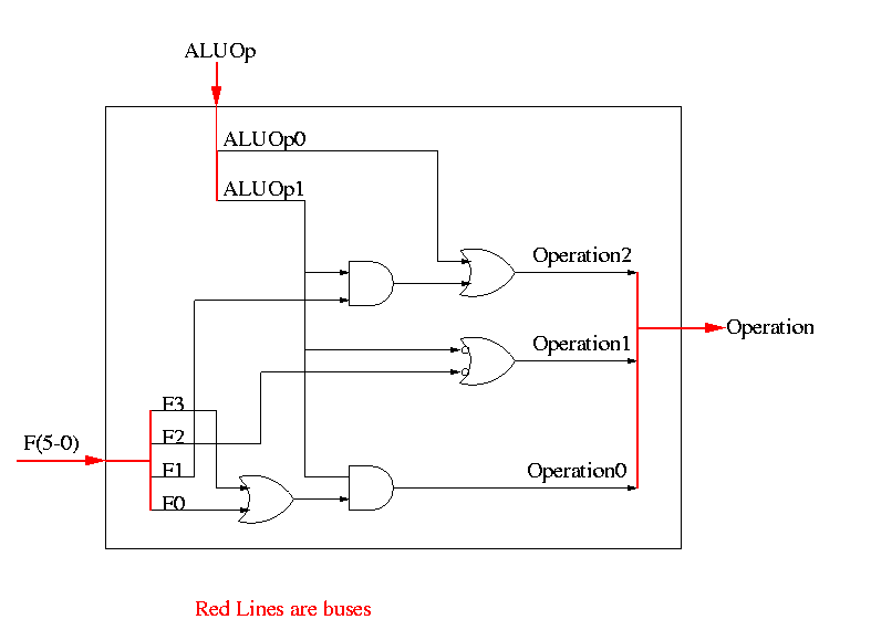
We need to generate the three ALU cntl lines: 1-bit Bnegate and 2-bit OP
    And     0 00
    Or      0 01
    Add     0 10
    Sub     1 10
    Set-LT  1 11
Homework:
What happens if we use 1 00? if we use 1 01?
Ignore the funny business in the HOB.
The funny business ``ruins'' these ops.
What information can we use to decide on the muxes and alu cntl lines?
The instruction!
So no problem, just do a truth table.
We will let the main control (to be done later) ``summarize'' the opcode for us. It will generate a 2-bit field ALUop
    ALUop   Action needed by ALU

    00      Addition (for load and store)
    01      Subtraction (for beq)
    10      Determined by funct field (R-type instruction)
    11      Not used
How many entries do we have now in the truth table
| opcode | ALUop | operation | funct field | ALU action | ALU cntl |
|---|---|---|---|---|---|
| LW | 00 | load word | xxxxxx | add | 010 |
| SW | 00 | store word | xxxxxx | add | 010 |
| BEQ | 01 | branch equal | xxxxxx | subtract | 110 |
| R-type | 10 | add | 100000 | add | 010 |
| R-type | 10 | subtract | 100010 | subtract | 110 |
| R-type | 10 | AND | 100100 | and | 000 |
| R-type | 10 | OR | 100101 | or | 001 |
| R-type | 10 | SLT | 101010 | set on less than | 111 |
    ALUop | Funct        ||  Bnegate:OP
    1 0   | 5 4 3 2 1 0  ||  B OP
    ------+--------------++------------
    0 0   | x x x x x x  ||  0 10
    x 1   | x x x x x x  ||  1 10
    1 x   | x x 0 0 0 0  ||  0 10
    1 x   | x x 0 0 1 0  ||  1 10
    1 x   | x x 0 1 0 0  ||  0 00
    1 x   | x x 0 1 0 1  ||  0 01
    1 x   | x x 1 0 1 0  ||  1 11
        ALUop | Funct
        1 0   | 5 4 3 2 1 0
        ------+------------
        x 1   | x x x x x x
        1 x   | x x 0 0 1 0
        1 x   | x x 1 0 1 0
        ALUop | Funct
        1 0   | 5 4 3 2 1 0
        ------+-------------
        x 1   | x x x x x x
        1 x   | x x x x 1 x
        ALUop | Funct
        1 0   | 5 4 3 2 1 0
        ------+------------
        0 0   | x x x x x x
        x 1   | x x x x x x
        1 x   | x x 0 0 0 0
        1 x   | x x 0 0 1 0
        1 x   | x x 1 0 1 0
        ALUop | Funct
        1 0   | 5 4 3 2 1 0
        ------+------------
        0 0   | x x x x x x
        x 1   | x x x x x x
        1 x   | x x x 0 x x
        ALUop | Funct
        1 0   | 5 4 3 2 1 0
        ------+------------
        0 x   | x x x x x x
        1 x   | x x x 0 x x
        ALUop | Funct
        1 0   | 5 4 3 2 1 0
        ------+------------
        0 x   | x x x x x x
        x x   | x x x 0 x x
        ALUop | Funct
        1 0   | 5 4 3 2 1 0
        ------+------------
        1 x   | x x 0 1 0 1
        1 x   | x x 1 0 1 0
        ALUop | Funct
        1 0   | 5 4 3 2 1 0
        ------+------------
        1 x   | x x x x x 1
        1 x   | x x 1 x x x
The circuit is then easy.
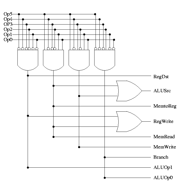
Now we need the main control
So 9 bits
The following figure shows where these occur.
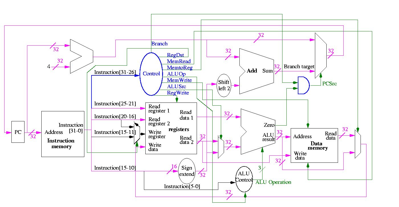
They all are determined by the opcode
The MIPS instruction set is fairly regular. Most fields we need are always in the same place in the instruction.
| MemRead: | Memory delivers the value stored at the specified addr |
| MemWrite: | Memory stores the specified value at the specified addr |
| ALUSrc: | Second ALU operand comes from (reg-file / sign-ext-immediate) |
| RegDst: | Number of reg to write comes from the (rt / rd) field |
| RegWrite: | Reg-file stores the specified value in the specified register |
| PCSrc: | New PC is Old PC+4 / Branch target |
| MemtoReg: | Value written in reg-file comes from (alu / mem) |
We have seen the wiring before (and given a hardcopy handout)
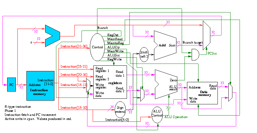
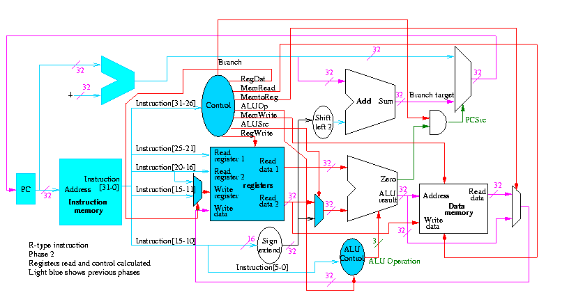
We are interested in four opcodes
Do a stage play
add r9,r5,r1 r9=r5+r1   0   5   1   9   0  32
sub r9,r9,r6            0   9   6   9   0  34
beq r9,r0,-8            4   9   0   <  -2   >
slt r1,r9,r0            0   9   0   1   0  42
lw  r1,102(r2)         35   2   1   <  100  >
sw  r9,102(r2)
The following figures illustrate the play.
We start with R-type instructions


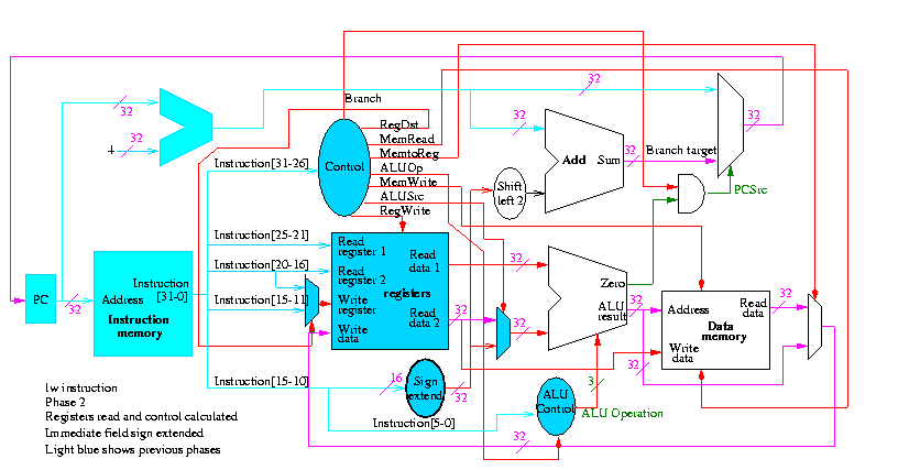
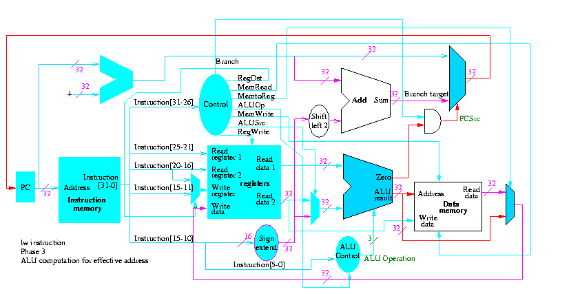
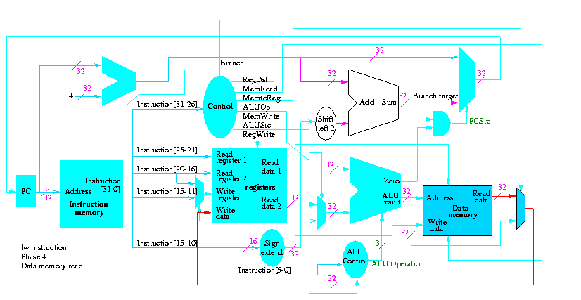
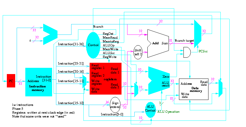
Next we show lw


The following truth table shows the settings for the control lines for each opcode. This is drawn differently since the labels of what should be the columns are long (e.g. RegWrite) and it is easier to have long labels for rows.
| Signal | R-type | lw | sw | beq |
|---|---|---|---|---|
| Op5 | 0 | 1 | 1 | 0 |
| Op4 | 0 | 0 | 0 | 0 |
| Op3 | 0 | 0 | 1 | 0 |
| Op2 | 0 | 0 | 0 | 1 |
| Op1 | 0 | 1 | 1 | 0 |
| Op0 | 0 | 1 | 1 | 0 |
| RegDst | 1 | 0 | X | X |
| ALUSrc | 0 | 1 | 1 | 0 |
| MemtoReg | 0 | 1 | X | X |
| RegWrite | 1 | 1 | 0 | 0 |
| MemRead | 0 | 1 | 0 | 0 |
| MemWrite | 0 | 0 | 1 | 0 |
| Branch | 0 | 0 | 0 | 1 |
| ALUOp1 | 1 | 0 | 0 | 0 |
| ALUOp | 0 | 0 | 0 | 1 |
Now it is straightforward but tedious to get the logic equations
When drawn in pla style the circuit is
Homework: 5.5 and 5.11 control, 5.1, 5.2, 5.10 (just the single-cycle datapath) 5.11
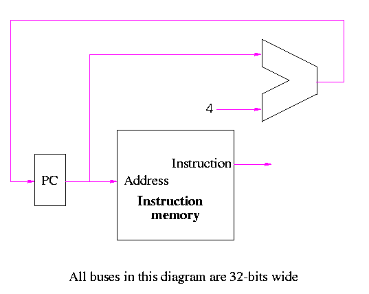
    opcode  addr
    31-26   25-0
Addr is word address; bottom 2 bits of PC are always 0
Top 4 bits of PC stay as they were (AFTER incr by 4)
Easy to add.
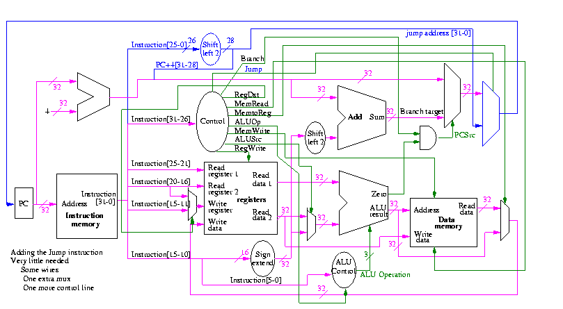
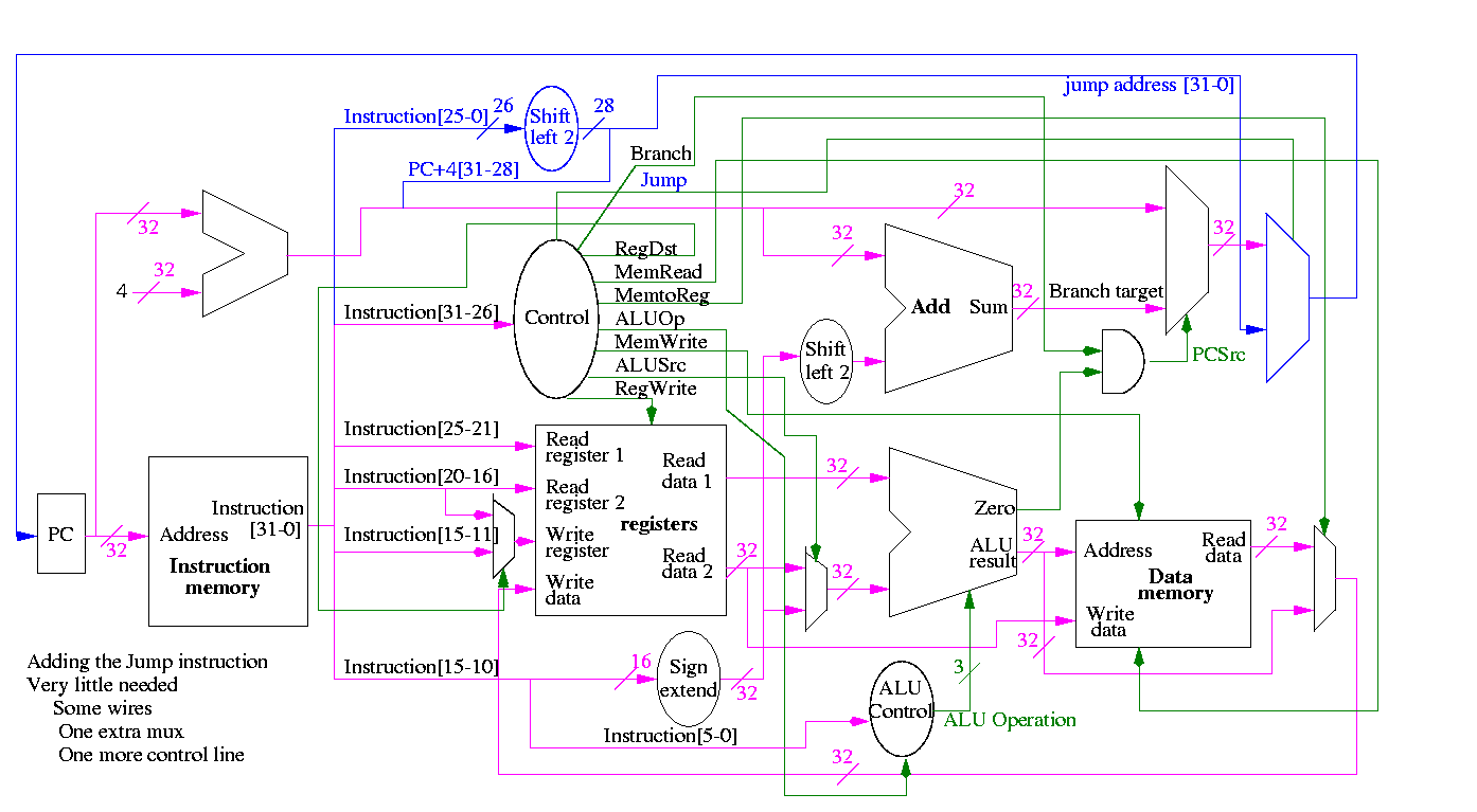
Smells like a good final exam type question.
Some instructions are likely slower than others and we must set the clock cycle time long enough for the slowest. The disparity between the cycle times needed for different instructions is quite significant when one considers implementing more difficult instructions, like divide and floating point ops.
Possible solutions
Even Faster
Homework: Read Chapter 2
Throughput measures the number of jobs per day that can be accomplished. Response time measures how long an individual job takes.
Performance = 1 / Execution time
So machine X is n times faster than Y means that
How should we measure execution-time?
We mostly use CPU time, but this does not mean the other metrics are worse.
Cycle time vs. Clock rate
So the execution time for a given job on a given computer is
(CPU) execution time = (#CPU clock cycles required) * (cycle time)
                     = (#CPU clock cycles required) / (Clock rate)
So a machine with a 10ns cycle time runs at a rate of
1 cycle per 10 ns = 100,000,000 cycles per second = 100 MHz
The number of CPU clock cycles required equals the number of instructions executed times the number of cycles in each instruction.
But systems are more complicated than that!
Through a great many measurement, one calculates for a given machine the average CPI (cycles per instruction).
#instructions for a given program depends on the instruction set. For example we saw in chapter 3 that 1 vax instruction is often accomplishes more than 1 MIPS instruction.
Complicated instructions take longer; either more cycles or longer cycle time
Older machines with complicated instructions (e.g. VAX in 80s) had CPI>>1
With pipelining can have many cycles for each instruction but still have CPI nearly 1.
Modern superscalar machines have CPI < 1
Putting this together, we see that
   Time (in seconds) =  #Instructions * CPI * Cycle_time (in seconds)
   Time (in ns) =  #Instructions * CPI * Cycle_time (in ns)
Homework: Carefully go through and understand the example on page 59
Homework: 2.1-2.5 2.7-2.10
Homework: Make sure you can easily do all the problems with a rating of [5] and can do all with a rating of [10]
What about MIPS?
Homework: Carefully go through and understand the example on pages 61-3
Why not use MFLOPS
Benchmarks
Homework: Carefully go through and understand 2.7 ``fallacies and pitfalls''
Ideal memory is
We observe empirically
So use a memory hierarchy
There is a gap between each pair of adjacent levels. We study the cache <---> memory gap
A cache is a small fast memory between the processor and the main memory. It contains a subset of the contents of the main memory.
A Cache is organized in units of blocks. Common block sizes are 16, 32, and 64 bytes.
A hit occurs when a memory reference is found in the upper level of memory hierarchy.
We start with a very simple cache organization.
Example on pp. 547-8.
| Address(10) | Address(2) | hit/miss | block# |
|---|---|---|---|
| 22 | 10110 | miss | 110 |
| 26 | 11010 | miss | 010 |
| 22 | 10110 | hit | 110 |
| 26 | 11010 | hit | 010 |
| 16 | 10000 | mis | 000 |
| 3 | 00011 | miss | 011 |
| 16 | 10000 | hit | 000 |
| 18 | 10010 | miss | 010 |
The basic circuitry for this simple cache to determine hit or miss and to return the data is quite easy.
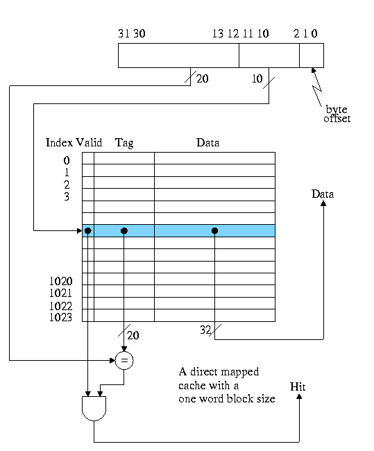
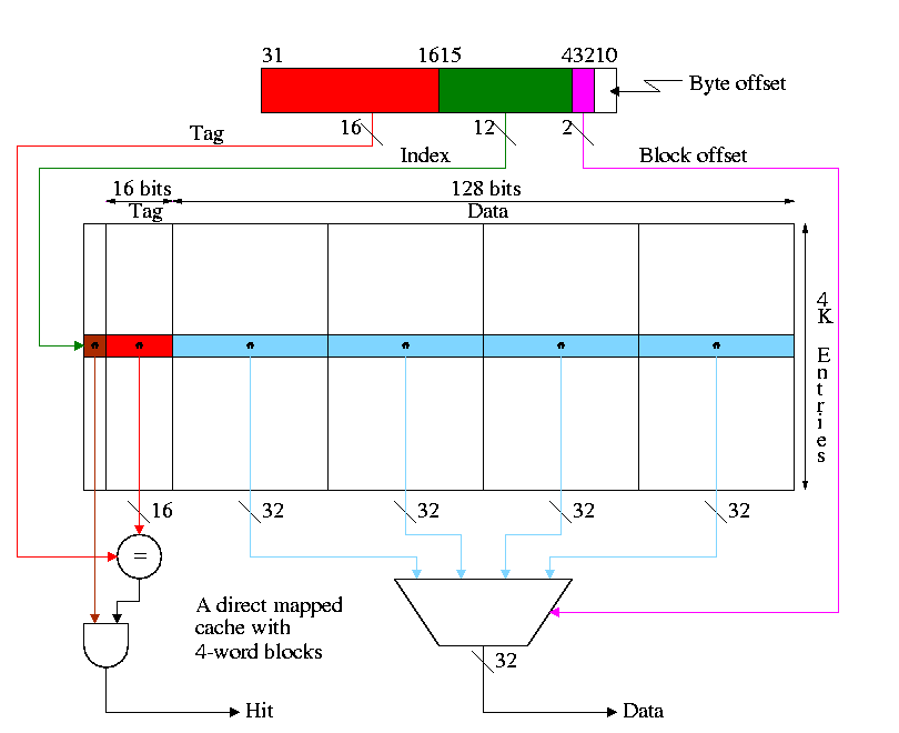
Calculate on the board the total number of bits in this cache.
Homework: 7.1 7.2 7.3
Processing a read for this simple cache
Skip section ``handling cache misses'' as it discusses the multicycle and pipelined implementations of chapter 6, which we skipped.
For our single cycle processor implementation we just need to note a few points
Homework: 7.2 7.3 (should have been give above with 7.1. I changed the notes so this is fix for ``next time'')
Homework: 7.7 7.8 7.9
Why not make blocksize enormous? Cache one huge block.
Homework: 7.11
Performance example to do on the board (dandy exam question).
Homework: 7.15, 7.16
A lower base (i.e. miss-free) CPI makes stalls appear more expensive since waiting a fixed amount of time for the memory corresponds to losing more instructions if the CPI is lower.
Faster CPU (i.e., a faster clock) makes stalls appear more expensive since waiting a fixed amount of time for the memory corresponds to more cycles if the clock is faster (and hence more instructions since the base CPI is the same).
Another performance example
Remark: Larger caches have longer hit times.
Consider the following sad story. Jane had a cache that held 1000 blocks and had a program that only references 4 (memory) blocks, namely 23, 1023, 123023, and 7023. In fact the reference occur in order: 23, 1023, 123023, 7023, 23, 1023, 123023, 7023, 23, 1023, 123023, 7023, 23, 1023, 123023, 7023, etc. Referencing only 4 blocks and having room for 1000 in her cache, Jane expected an extremely high hit rate for her program. In fact, the hit rate was zero. She was so sad, she gave up her job as webmistriss, went to medical school, and is now a brain surgeon at the mayo clinic in rochester MN.
We continue to assume a byte addressed machines, but all references are to a 4-byte word (lw and sw).
The 2 LOBs are not used (they specify the byte within the word but all our references are for a complete word). We show these two bits in dark blue. We continue to assume 32 bit addresses so there are 2**30 words in the address space.
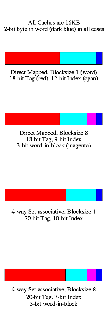
Let's review various possible cache organizations and determine for each how large is the tag and how the various address bits are used. We will always use a 16KB cache. That is the size of the data portion of the cache is 16KB = 4 kilowords = 2**12 words.
Homework: 7.39, 7.40 (not assigned 1999-2000)
Modern high end PCs and workstations all have at least two levels of caches: A very fast, and hence not too big, first level (L1) cache together with a larger but slower L2 cache.
When a miss occurs in L1, L2 is examined and only if a miss occurs there is main memory referenced.
So the average miss penalty for an L1 miss is
(L2 hit rate)*(L2 time) + (L2 miss rate)*(L2 time + memory time)We are assuming L2 time is the same for an L2 hit or L2 miss. We are also assuming that the access doesn't begin to go to memory until the L2 miss has occurred.
Do an example
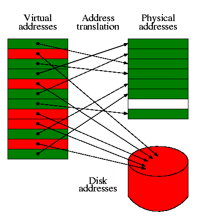
I realize this material was covered in operating systems class (V22.0202). I am just reviewing it here. The goal is to show the similarity to caching, which we just studied. Indeed, (the demand part of) demand paging is caching: In demand paging the memory serves as a cache for the disk, just as in caching the cache serves as a cache for the memory.
The names used are different and there are other differences as well.
| Cache concept | Demand paging analogue |
|---|---|
| Memory block | Page |
| Cache block | Page Frame (frame) |
| Blocksize | Pagesize |
| Tag | None (table lookup) |
| Word in block | Page offset |
| Valid bit | Valid bit |
| Cache concept | Demand paging analogue |
|---|---|
| Associativity | None (fully associative) |
| Miss | Page fault |
| Hit | Not a page fault |
| Miss rate | Page fault rate |
| Hit rate | 1 - Page fault rate |
| Placement question | Placement question |
| Replacement question | Replacement question |
Homework: 7.39, 7.40 (should have been asked earlier)
Homework: 7.32
Question: On a write hit should we write the new value through to (memory/disk) or just keep it in the (cache/memory) and write it back to (memory/disk) when the (cache-line/page) is replaced.
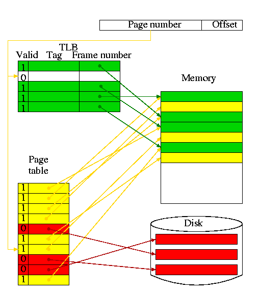
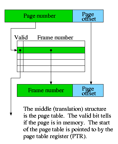
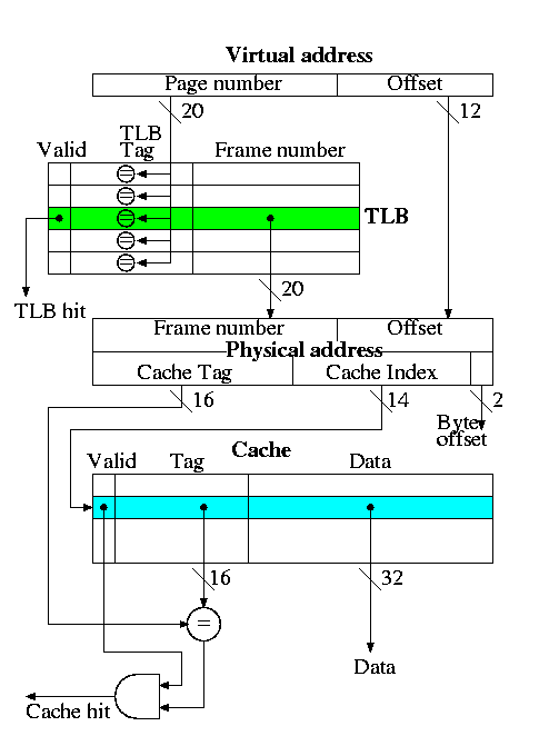
A TLB is a cache of the page table
This is the decstation 3100
Actions taken
| TLB | Page | Cache | Remarks |
|---|---|---|---|
| hit | hit | hit | Possible, but page table not checked on TLB hit, data from cache |
| hit | hit | miss | Possible, but page table not checked, cache entry loaded from memory |
| hit | miss | hit | Impossible, TLB references in-memory pages |
| hit | miss | miss | Impossible, TLB references in-memory pages |
| miss | hit | hit | Possible, TLB entry loaded from page table, data from cache |
| miss | hit | miss | Possible, TLB entry loaded from page table, cache entry loaded from memory |
| miss | miss | hit | Impossible, cache is a subset of memory |
| miss | miss | miss | Possible, page fault brings in page, TLB entry loaded, cache loaded |
Homework: 7.31, 7.33
This could be called the placement question. There is another placement question in OS memory memory management. When dealing with varying size pieces (segmentation or whole program swapping), the available space becomes broken into varying size available blocks and varying size allocated blocks (called holes). We do not discussing the above placement question in this course (but presumably it was in 204 when you took it and for sure it will be in 204 next semester--when I teach it).
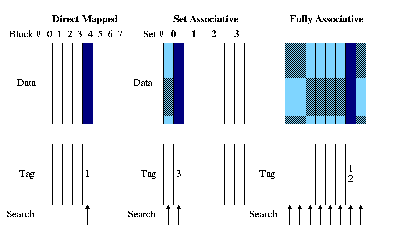
The placement question we do study is the associativity of the structure.
Assume a cache with N blocks
| Feature | Typical values for caches |
Typical values for paged memory |
Typical values for TLBs |
|
| Size | 8KB-8MB | 16MB-2GB | 256B-32KB | |
| Block size | 16B-256B | 4KB-64KB | 4B-32B | |
| Miss penalty in clocks | 10-100 | 1M-10M | 10-100 | |
| Miss rate | .1%-10% | .000001-.0001% | .01%-2% |
| Associativity | Location method | Comparisons Required |
|---|---|---|
| Direct mapped | Index | 1 |
| Set Associative | Index the set, search among elements | Degree of associativity |
| Full | Search all cache entries | Number of cache blocks |
| Separate lookup table | 0 |
The difference in sizes and costs for demand paging vs. caching, leads to a different choice implementation of finding the block. Demand paging always uses the bottom row with a separate table (page table) but caching never uses such a table.
This is called the replacement question and is much studied in demand paging (remember back to 202).
Homework: 7.41
With processor speed increasing 50% / year, I/O must improved or essentially all jobs will be I/O bound.
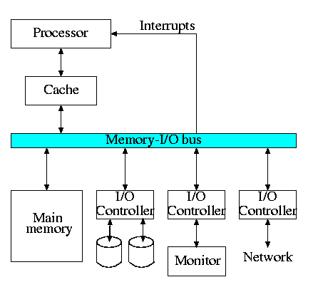
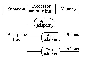
The diagram on the right is quite oversimplified for modern PCs but serves the purpose of this course.
Devices are quite varied and their datarates vary enormously.
Show a real disk opened up and illustrate the components
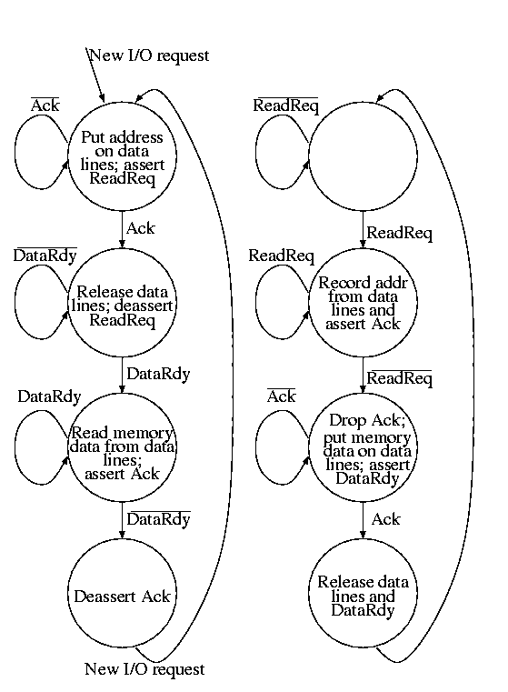
A bus is a shared communication link, using one set of wires to connect many subsystems.
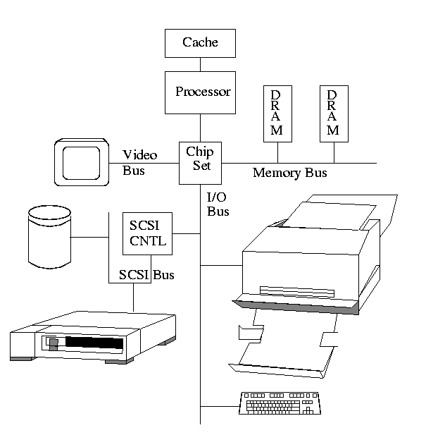
A synchronous bus is clocked.
An asynchronous bus is not clocked.
These improvements mostly come at the cost of increased expense and/or complexity.
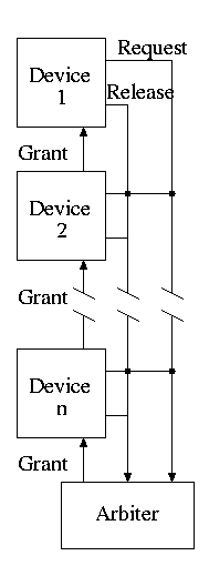
| Option | High performance | Low cost |
|---|---|---|
| bus width | separate address and data lines | multiplex address and data lines |
| data width | wide | narrow |
| transfer size | multiple bus loads | single bus loads |
| bus masters | multiple | single |
| clocking | synchronous | asynchronous |
Do on the board the example on pages 665-666
This is really an OS issue. Must write/read to/from device registers, i.e. must communicate commands to the controller.
Should we check periodically or be told when there is something to do? Better yet can we get someone else to do it since we are not needed for the job?
Processor continually checks the device status to see if action is required.
Do on the board the example on pages 676-677
Processor is told by the device when to look. The processor is interrupted by the device.
Do on the board the example on pages 681-682
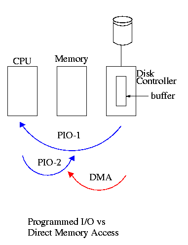
The processor initiates the I/O operation then ``something else'' takes care of it and notifies the processor when it is done (or if an error occurs).